
Owner manual
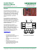

Digilent, Inc.
Cerebot Nano Reference Manual
www.digilentinc.com page 6 of 6
Copyright Digilent, Inc. All rights reserved. Other product and company names mentioned may be trademarks of their respective owners.
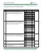
All Pmod connector pins can be used for general purpose I/Os. The following table describes how the
Cerebot Nano header pins connect to ATmega168 ports/bits.
DESCRIPTION PIN FUNCTION PORT/BIT
JA Analog Input and PmodHB5 Connections
JA1 through JA4 can be used as analog inputs in
applications and pins JA7 through JA10 are ideally suited
for connection with a Digilent PmodHB5 motor control
board.
1 ADC0/PCINT8 PC0
2 ADC1/PCINT9 PC1
3 ADC2/PCINT10 PC2
4 ADC3/PCINT11 PC3
5 GND
6 VCC
7 INT0/PCINT18 PD2
8 OC1A/PCINT1 PB1
9 ICP1/PCINT0 PB0
10
INT1/PCINT19 PD3
11
GND
12
VCC
JB Serial Communication and General I/O
Pins JB1 through JB4 provide access to the TWI and
USART communication interfaces. Pins JB7 and JB10 are
limited to general I/O and JB8 and JB9 provide access to
the output compare pins of Timer/Counter 0.
1 ADC5/SCL/PCIN
T13
PC5
2 ADC4/SDA/PCIN
T12
PC4
3 RXD/PCINT16 PD0
4 TXD/PCINT17 PD1
5 GND
6 VCC
7 XCK/T0/PCINT20
PD4
8 T1/OC0B/PCINT
21
PD5
9 AIN0/OC0A/PCIN
T22
PD6
10
AIN1/PCINT23 PD7
11
GND
12
VCC
J1 SPI Interface and In-System Programming
When the shorting block on JP1 is in the SS position, J1 is
used for the SPI port. When the shorting block on JP1 is in
the RST position, J1 is used for in-system programming.
1 PCINT2/SS/OC1
B
PB2
2 PCINT3/OC2A/M
OSI
PB3
3 PCINT4/MISO PB4
4 SCK/PCINT5 PB5
5 GND
6 VCC
J2 TWI Connectors
The Atmel TWI interface can be accessed on this
connector.
1 ADC5/SCL/PCIN
T13
PC5
2 ADC4/SDA/PCIN
T12
PC4
J4 ADC Input Only
Analog to digital input channels 6 and 7 are input-only and
have digital I/O capabilities.
1 ADC6
2 ADC7