
International User's Manual Network Adapter RCM4000


User’s Manual 87
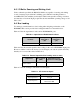
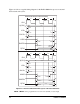
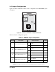
Table A-8 lists the delays in gross memory access time for several values of VDD
IO
.
The measurements are taken at the 50% points under the following conditions.
• T = -40°C to 85°C, V = VDD
IO
±10%
• Internal clock to nonloaded CLK pin delay ≤ 1 ns @ 85°C/3.0 V
The clock to address output delays are similar, and apply to the following delays.
• T
adr
, the clock to address delay
• T
CSx
, the clock to memory chip select delay
• T
IOCSx
, the clock to I/O chip select delay
• T
IORD
, the clock to I/O read strobe delay
• T
IOWR
, the clock to I/O write strobe delay
• T
BUFEN
, the clock to I/O buffer enable delay
The data setup time delays are similar for both T
setup
and T
hold
.
When the spectrum spreader is enabled with the clock doubler, every other clock cycle is
shortened (sometimes lengthened) by a maximum amount given in the table above. The
shortening takes place by shortening the high part of the clock. If the doubler is not
enabled, then every clock is shortened during the low part of the clock period. The maxi-
mum shortening for a pair of clocks combined is shown in the table.
Technical Note TN227, Interfacing External I/O with Rabbit Microprocessor Designs,
contains suggestions for interfacing I/O devices to the Rabbit 4000 microprocessors.
Table A-8. Preliminary Data and Clock Delays
VDD
IO
(V)
Clock to Address
Output Delay
(ns)
Data Setup
Time Delay
(ns)
Worst-Case
Spectrum Spreader Delay
(ns)
30 pF 60 pF 90 pF
0.5 ns setting
no dbl / dbl
1 ns setting
no dbl / dbl
2 ns setting
no dbl / dbl
3.3 6 8 11 1 2.3 / 2.3 3 / 4.5 4.5 / 9
1.8 18 24 33 3 7 / 6.5 8 / 12 11 / 22