
International User's Manual Network Adapter RCM4000


36 RabbitCore RCM4000
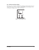
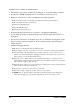
If a device such as a battery is
connected across two channels
for a differential measurement,
and it is not referenced to
analog ground, then the current
from the device will flow
through both sets of attenuator
resistors as shown in Figure 11.
This will generate a negative
voltage at one of the inputs,
LN1, which will almost cer-
tainly lead to inaccurate A/D
conversions. To make such dif-
ferential measurements, connect the R1 resistors to the A/D converter’s internal reference
voltage, which is software-configurable for 1.15 V, 2.048 V, or 2.5 V. This internal reference
voltage is available on pin 49 of header J3 as VREF, and allows you to convert analog
input voltages that are negative with respect to analog ground.
NOTE: The amplifier inside the A/D converter’s internal voltage reference circuit has a
very limited output-current capability. The internal buffer can source up to 20 mA and
sink only up to 20 µA. Use a separate buffer amplifier if you need to supply any load
current.
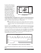
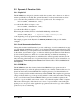
The A/D converter’s CONVERT pin is available on pin 48 of header J3 and can be used as
a hardware means of forcing the A/D converter to start a conversion cycle. The CONVERT
signal is an edge-triggered event and has a hold time of two CCLK periods for debounce.
A conversion is started by an active (rising) edge on the CONVERT pin. The CONVERT
pin must stay low for at least two CCLK periods before going high for at least two CCLK
periods. Figure 12 shows the timing of a conversion start. The double falling arrow on
CCLK indicates the actual start of the conversion cycle.
Figure 12. Timing Diagram for Conversion Start Using CONVERT Pin
Appendix B explains the implementation examples of these features on the Prototyping
Board.
Figure 11. Current Flow from Ungrounded
or Floating Source
R5
R6
2.2 nF
R14
R13
2.2 nF
ADC
AIN0
AIN1
+
I
LN0
LN1
+
-
Device
CCLK
BUSY
CONV
Conversion starts