
International Computer Hardware User Manual


Clock timing
838
NS9750 Hardware Reference
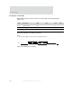
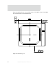
LCD input clock timing
Table 482 describes the values shown in the LCD input clock timing diagram
(Figure 147).
Note:
1 The clock rate supplied on lcdclk is twice the actual LCD clock rate.
Figure 147: LCD input clock timing
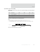
Parm Description Min Max Unit Notes
LC1 lcdclk cycle time 6.25 ns 1
LC2 lcdclk high time (LC1/2) x 0.4 (LC1/2) x 0.6 ns
LC3 lcdclk low time (LC1/2) x 0.4 (LC1/2) x 0.6 ns
Table 482: LCD input clock timing parameters
LC2
LC1
LC2 LC3
LC1
LC3
lcdclk