PROMETHEUS™ High Integration PC/104 CPU with Ethernet and Data Acquisition Models PR-Z32-E-ST, PR-Z32-EA-ST User Manual V1.44 Copyright 2003 Diamond Systems Corporation 8430-D Central Ave. Newark, CA 94560 Tel (510) 456-7800 www.diamondsystems.
PROMETHEUS High-Integration PC/104 CPU with Ethernet and Data Acquisition TABLE OF CONTENTS 1. DESCRIPTION ......................................................................................................................4 2. FEATURES ...........................................................................................................................5 3. PROMETHEUS BOARD DRAWING ....................................................................................7 4. I/O HEADERS ..........
19. DIGITAL I/O OPERATION ..................................................................................................58 20. COUNTER/TIMER OPERATION ........................................................................................59 21. DATA ACQUISITION SPECIFICATIONS...........................................................................62 22. FLASHDISK MODULE .......................................................................................................63 22.2 22.3 22.
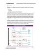
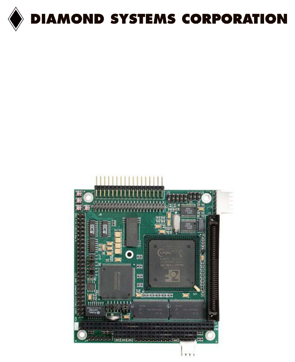
PROMETHEUS High-Integration PC/104 CPU with Ethernet and Data Acquisition 1. DESCRIPTION Prometheus is an embedded PC/104 CPU that integrates 3 separate circuits onto a single compact board: ♦ CPU ♦ Ethernet ♦ Analog I/O (optional, model PR-Z32-EA only) A detailed list of features is shown on the next page. Prometheus conforms to the PC/104 standard, an embedded standard that is based on the ISA and PCI buses and provides a compact, rugged mechanical design for embedded systems.
2. FEATURES System Features Processor Section ♦ 486-DX2 processor running at 100MHz with co-processor ♦ Pentium class platform including burst-mode SDRAM and PCI-based IDE controller and USB ♦ 32MB SDRAM system memory ♦ 50MHz memory bus for improved performance ♦ 2MB 16-bit wide integrated flash memory for BIOS and user programs ♦ 8KB unified level 1 cache I/O ♦ 4 serial ports, 115.
Data Acquisition Subsystem (Model PR-Z32-EA Only) Analog Input ♦ 16 single-ended / 8 differential inputs, 16-bit resolution ♦ 100KHz maximum aggregate A/D sampling rate ♦ Programmable input ranges/gains with maximum range of ±10V / 0-10V ♦ Both bipolar and unipolar input ranges ♦ 5 ppm/oC drift accuracy ♦ Internal and external A/D triggering ♦ 48-sample FIFO for reliable high-speed sampling and scan operation Analog Output ♦ 4 analog outputs, 12-bit resolution ♦ ±10V and 0-10V output ranges
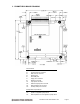
3.
4. I/O HEADERS All cables mentioned in this chapter are included in Diamond Systems’ cable kit C-PRZ-KIT. These cables are further described in chapter 25. Some cables are also available individually. 4.
Notes on J3 Signals COM1 – COM4 The signals on these pins are RS-232 level signals and may be connected directly to RS-232 devices. The pinout of these signals is designed to allow a 9-pin male IDC connector to be crimped onto the corresponding ribbon cable wires to provide the correct pinout for a PC serial port connector (DTE). LPT1 The signals on these pins comprise a standard PC parallel port.
4.2 Input Power – J11 1 2 3 4 5 6 7 8 9 +5V In Ground Ground +12V In Ground +5V In -12V In -5V In ATX Control Input power for Prometheus may be supplied either through J11 from an external supply or directly through the PC/104 bus power pins if a PC/104 power supply is used with the CPU. Prometheus requires only +5VDC input power to operate. All other required voltages are generated on board with miniature switching regulators.
4.3 Output Power – J12 1 2 3 4 +5V Out Ground Ground +12V Out J12 provides switched power for use with external drives. If ATX is enabled, the power is switched on and off with the ATX input switch. If ATX is not enabled, the power is switched on and off in conjunction with the external power. Diamond Systems’ cable no. 698006 mates with J12. It provides a standard full-size power connector for a hard drive or CD-ROM drive and a standard miniature power connector for a floppy drive. 4.
4.6 Auxiliary Serial Port Connector – J15 1 2 3 4 5 6 RX COM1 TX COM1 Ground RX COM2 TX COM2 Ground Pin 2 on DB9 #1 Pin 3 on DB9 #1 Pin 5 on DB9 #1 Pin 2 on DB9 #2 Pin 3 on DB9 #2 Pin 5 on DB9 #2 This 6-pin header is provided for auxiliary access to serial ports 1 and 2 with signals RX, TX, and Ground for each port. This connector may be used in low-cost limited I/O configurations as an alternative to the 80-pin connector J3. Do not use both J15 and the corresponding pins on J3 simultaneously.
4.8 Floppy Drive – J7 Ground Ground Ground Ground Ground Ground Ground Ground Ground Ground Ground Ground Ground Ground Ground Ground Ground 1 3 5 7 9 11 13 15 17 19 21 23 25 27 29 31 33 2 4 6 8 10 12 14 16 18 20 22 24 26 28 30 32 34 High Density Unused Unused Index Motor Enable Drive Select B Drive Select A Motor Enable Direction Step Write Data Write Enable Track 0 Write Protect Read Data Select Protect Disk Change J7 is a 2x17 pin header. It mates with Diamond Systems’ cable no.
4.10 Data Acquisition I/O Connector – J14 (Model PR-Z32-EA only) Prometheus model PR-Z32-EA includes a 50-pin header labeled J14 for all data acquisition I/O. This header is located on the left side of the board. Pin 1 is the lower right pin and is marked on the board. Diamond Systems’ cable no. C-50-18 provides a standard 50-pin connector at each end and mates with this header.
4.11 PC/104 Bus Connectors The PC/104 bus is essentially identical to the ISA Bus except for the physical design. It specifies two pin and socket connectors for the bus signals. A 64-pin header J1 incorporates the 62-pin 8bit bus connector signals, and a 40-pin header J2 incorporates the 36-pin 16-bit bus connector signals. The additional pins on the PC/104 connectors are used as ground or key pins.
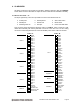
5. JUMPER CONFIGURATION Refer to the Prometheus board drawing on page 7 for locations of the configuration items mentioned here. Also see page 45 for information on configuration J13 for the data acquisition circuit. 5.1 J10: System Configuration Jumper block J10 is used for configuration of IRQ levels, wait states, ATX power control, and CMOS RAM. Serial Port and A/D IRQ Settings COM3 may be set to IRQ4 or IRQ9. COM4 may be set to IRQ3 or IRQ15.
The different configurations for J10 are shown below. Each illustration shows only the jumper of interest. An asterisk (*) indicates the default setting. 5.2 J6: Watchdog Timer & System Recovery J6 is used to configure the watchdog timer and enable system recovery (failsafe mode) in case of BIOS corruption. This jumper has different dimensions than J10 and J13, and the jumpers are not interchangeable. Watchdog timer operation is described in detail on page 20.
6. SYSTEM FEATURES 6.1 System Resources The table below lists the default system resources utilized by the circuits on Prometheus. Device Address (Hex) IRQ DMA Serial Port COM1 I/O 3F8-3FF 4 - Serial Port COM2 I/O 2F8 – 2FF 3 - Serial Port COM3 I/O 3E8 – 3EF 4 - Serial Port COM4 I/O 2E8 – 2EF 3 - Parallel Port LPT1 I/O 378 – 37F 7 3 IDE Controller I/O 1F0 – 1F7 14 - Floppy Controller - A/D Circuit (PR-Z32-EA only) I/O 280 – 28F 5 - Ethernet I/O 1000 10 - 11 - USB 6.
6.3 Console Redirection to a Serial Port In many applications without a video card it may be necessary to obtain keyboard and monitor access to the CPU for configuration, file transfer, or other operations. Prometheus supports this operation by enabling keyboard input and character output onto a serial port (console redirection).
6.4 Watchdog Timer Prometheus contains a watchdog timer circuit consisting of two programmable timers, WD1 and WD2, cascaded together. The input to the circuit is WDI, and the output is WDO. Both signals appear on I/O connector WDI may be triggered in hardware or in software. A special “early” version of WDO may be output on the WDO pin. When this signal is connected to WDI, the watchdog circuit will be retriggered automatically.
6.5 Failsafe Mode / BIOS Recovery The ZFx86 failsafe feature consists of a small command interpreter built in to the ZFx86 CPU chip. The ZFx86 contains a ROM with the command interpreter as well as an 8KB RAM. It may be used to power up the system and download the BIOS to recover from situations in which the BIOS accidentally becomes corrupted or erased. The failsafe feature is used in the factory to program the BIOS in new Prometheus boards for the first time.
7. BIOS 7.1 BIOS Settings Prometheus uses a BIOS from Phoenix Technologies modified to support the custom features of the ZF Micro ZFx86 chip and the Prometheus board. Some of these features are described here. To enter the BIOS during system startup (POST – power on self-test), press F2. Serial Ports -The address and interrupt settings for serial ports COM1 – COM4 may be modified. COM1 and COM2 address and interrupt settings are done in the BIOS, Advanced menu, I/O Device Configuration.
7.2 BIOS Download / Recovery Because the BIOS is stored in reprogrammable Flash memory, it is possible that the BIOS could be accidentally erased when trying to write other files into the Flash. To recover from this situation the CPU chip on Prometheus contains a special failsafe Boot-Up ROM (BUR) that can be activated on power-up.
7.3 Disk-On-Board™ Flash File Storage Prometheus supports the use of its on-board flash memory as a disk drive. About 1.45Mbytes of the total 2MB capacity is available for this function. This valuable feature lets you run a DOS operating system right from the flash without having to use any external storage media in your finished application. You save the cost of external disk drives or flashdisk modules and associated cables and assembly time.
Known Limitations • RFD (onboard flash drive) is not compatible with DOS expanded memory configuration in EMM386.EXE. Use the NOEMS switch appended to the end of the EMM386 line in your config.sys to bypass EMS. Example line in config.sys: device=c:\DOS\EMM386.exe NOEMS • The onboard flash chip has a limitation of 2,000,000 erase cycles, so swap drives or virtual memory functions should not be used. • Currently we are shipping 2M byte Flash chips so Onboard Flash drives can be formatted with 1.
8. SYSTEM I/O 8.1 Ethernet Prometheus includes a 100Mbps Ethernet connection using 100BaseT wiring. The signals are provided on a 6-pin header J4 on the bottom edge of the board. Diamond Systems’ cable no. 698002 mates with this header and provides a standard RJ-45 connector in panel-mount form for connecting to standard Cat5 network cables. 1 2 3 4 5 6 Common RXCommon RX+ TXTX+ J4 – Ethernet Connector The Ethernet chip is the National Semiconductor DP83815 MacPhyter chip.
8.2 Serial Ports Prometheus contains 4 serial ports. Each port is capable of transmitting at speeds of up to 115.2Kbaud. Ports COM1 and COM2 are built into the ZF Micro CPU chip. They consist of standard 16550 type UARTs with 16-byte FIFOs. Ports COM3 and COM4 are derived from an Exar 16C2850 dual UART chip and include 128-byte FIFOs. Ports 3 and 4 may be operated at speeds up to 1.5Mbaud with installation of high-speed drivers as a custom option.
9. NOTES ON OPERATING SYSTEMS AND BOOTING PROCEDURES 9.1 Booting to DOS From a Floppy Drive In some revisions of the ZF Micro processor chip and Phoenix BIOS on Prometheus, there is a short period of conflict between the floppy drive and the programmable chip selects during the booting from a floppy disk in certain operating systems such as Windows 98. This conflict makes it impossible to boot to DOS from a floppy disk with these chip selects enabled.
9.3 Installing an OS from a Hard Disk onto a Flashdisk Module To install an operating system such as DOS or VxWorks from a hard drive onto a flashdisk module, follow the procedure below. The process requires a floppy drive with a bootable DOS diskette, a hard disk with the operating system, the flashdisk module, the IDE extender board, and associated cables.
10. DATA ACQUISITION CIRCUIT Model PR-Z32-EA contains a data acquisition subsystem consisting of A/D, D/A, digital I/O, and counter/timer features. This subsystem is equivalent to a complete add-on data acquisition module. The A/D section includes a 16-bit A/D converter, 16 input channels, and a 48-sample FIFO. Input ranges are programmable, and the maximum sampling rate is 100KHz. The D/A section includes 4 12-bit D/A channels. The digital I/O section includes 24 lines with programmable direction.
11. DATA ACQUISITION CIRCUITRY I/O MAP 11.1 Base Address The data acquisition circuitry on Prometheus occupies a block of 16 bytes in I/O memory space. The default address range for this block is 280h – 28Fh (base address 280). This address should work for most applications, but it can be changed in the BIOS if necessary. Go to the Advanced screen and select Advanced Chipset Control, then ISA I/O Chip Select Setup. Scroll down to I/O Window io_cs3, which is used for the data acquisition circuit.
11.
11.3 Register Bit Definitions In these register definitions, a bit marked ‘X’ is an unused bit. All unused bits in readable registers read back as 0. Base + 0 Bit No. Name Write 7 Command Register 6 5 4 3 STRTAD RSTBRD RSTDA RSTFIFO CLRDMA 2 1 0 CLRT CLRD CLRA This register is used to perform various functions. The register bits are not data bits but instead command triggers. Each function is initiated by writing a 1 to a particular bit.
Base + 0 Read A/D LSB Bit No. 7 6 5 4 3 2 1 0 Name AD7 AD6 AD5 AD4 AD3 AD2 AD1 AD0 AD7 - 0 A/D data bits 7 - 0; AD0 is the LSB; A/D data is an unsigned 16-bit value. The A/D value is derived by reading two bytes from Base + 0 and Base + 1 and applying the following formula: A/D value = (Base + 0 value) + (Base + 1 value) * 256 The value is interpreted as a twos complement 16-bit number ranging from –32768 to +32767.
Base + 2 Read/Write A/D Channel Register Bit No. 7 6 5 4 3 2 1 0 Name H3 H2 H1 H0 L3 L2 L1 L0 H3 – H0 High channel of channel scan range Ranges from 0 to 15 in single-ended mode, 0 - 7 in differential mode. L3 - L0 Low channel of channel scan range Ranges from 0 to 15 in single-ended mode, 0 - 7 in differential mode. The high channel must be greater than or equal to the low channel.
Base + 3 Write Analog Input Gain Bit No. 7 6 5 4 3 2 1 0 Name X X X X X SCANEN G1 G0 SCANEN 1 Scan mode enable: Each A/D trigger will cause the board to generate an A/D conversion on each channel in the range LOW – HIGH (the range is set with the channel register in Base + 2). The STS bit (read Base + 3 bit 7) stays high during the entire scan. 0 Each A/D trigger will cause the board to generate a single A/D conversion on the current channel.
Base + 3 Read Analog Input Status Bit No. 7 6 5 4 3 2 1 0 Name STS SD WAIT DACBSY OVF SCANEN G1 G0 STS A/D status. 1 = A/D conversion or scan in progress, 0 = A/D is idle. If SCANEN = 0 (single conversion mode), STS goes high when an A/D conversion is started and stays high until the conversion is finished. If SCANEN = 1 (scan mode enabled), STS stays high during the entire scan.
Base + 4 Bit No. Name CKSEL1 Read/Write 7 Interrupt / DMA / Counter Control 6 5 4 CKSEL1 CKFRQ1 CKFRQ0 ADCLK 3 2 1 0 DMAEN TINTE DINTE AINTE Clock source selection for counter/timer 1: 0 = internal oscillator, frequency selected by CLKFRQ1 1 = external clock input CLK1 (DIO C pins must be set for ctr/timer signals) CKFRQ1 Input frequency selection for counter/timer 1 when CKSEL1 = 1: 0 = 10MHz, 1 = 100KHz CKFRQ0 Input frequency selection for counter/timer 0.
Base + 6 Write DAC LSB Bit No. 7 6 5 4 3 2 1 0 Name DA7 DA6 DA5 DA4 DA3 DA2 DA1 DA0 DA7–0 Base + 6 D/A data bits 7 - 0; DA0 is the LSB. D/A data is an unsigned 12-bit value. This register must be written to before Base + 7, since writing to Base + 7 updates the DAC immediately. Read A/D Channel and FIFO Status Bit No. 7 6 5 4 3 2 1 0 Name 0 0 FD5 FD4 FD3 FD2 FD1 FD0 FD5–0 Current FIFO depth.
Base + 7 Write DAC MSB + Channel No. Bit No. 7 6 5 4 3 2 1 0 Name DACH1 DACH0 X X DA11 DA10 DA9 DA8 DACH1–0 D/A channel. The value written to Base + 6 and Base + 7 are written to the selected channel, and that channel is updated immediately. The update takes approximately 20 microseconds due to the DAC serial interface. DA11–8 Base + 7 D/A bits 11 - 8; DA11 is the MSB. D/A data is an unsigned 12-bit value. Read Analog Operation Status Bit No.
Base + 8 Read / Write Digital I/O Port A Bit No. 7 6 5 4 3 2 1 0 Name A7 A6 A5 A4 A3 A2 A1 A0 Base + 9 Read / Write Digital I/O Port B Bit No. 7 6 5 4 3 2 1 0 Name B7 B6 B5 B4 B3 B2 B1 B0 Base + 10 Read / Write Digital I/O Port C Bit No. 7 6 5 4 3 2 1 0 Name C7 C6 C5 C4 C3 C2 C1 C0 These 3 registers are used for digital I/O. The direction of each register is controlled by bits in the register below.
Base + 12 Read/Write Counter/Timer D7 - 0 Bit No. 7 6 5 4 3 2 1 0 Name D7 D6 D5 D4 D3 D2 D1 D0 This register is used for both Counter 0 and Counter 1. It is the LSB for both counters. When writing to this register, an internal load register is loaded. Upon issuing a Load command through Base + 15, the selected counter’s LSB register will be loaded with this value. When reading from this register, the LSB value of the most recent Latch command will be returned.
Base + 15 Write Counter/Timer Control Register Bit No. 7 6 5 4 3 2 1 0 Name CTRNO LATCH GTDIS GTEN CTDIS CTEN LOAD CLR This register is used to control the counter/timers. A counter is selected with bit 7, and then a 1 is written to any ONE of bits 6 – 0 to select the desired operation for that counter. The other bits and associated functions are not affected. Thus only one operation can be performed at a time. CTRNO Counter no.
Base + 15 Read FPGA Revision Code Bit No. 7 6 5 4 3 2 1 0 Name REV7 REV6 REV5 REV4 REV3 REV2 REV1 REV0 This register is used to control the counter/timers. A counter is selected with bit 7, and then a 1 is written to any ONE of bits 6 – 0 to select the desired operation for that counter. The other bits and associated functions are not affected. Thus only one operation can be performed at a time. REV7-0 Revision code, read as a 2-digit hex value, i.e. 0x20 = revision 2.
12. DATA ACQUISITION CIRCUIT CONFIGURATION Jumper block J13 is used to configure the A/D and D/A circuits on PR-Z32-EA. It is located on the left side of the board next to the data acquisition I/O pin header and is oriented vertically. The functions are shown below and are described in detail on the following page. The default settings are as shown: The various configurations are illustrated and described below.
Single-ended / Differential Inputs Prometheus can accept both single-ended and differential inputs. A single-ended input uses 2 wires, input and ground. The measured input voltage is the difference between these two wires. A differential input uses 3 wires: input +, input -, and ground. The measured input voltage is the difference between the + and - inputs.
13. ANALOG INPUT RANGES AND RESOLUTION 13.1 Overview Prometheus uses a 16-bit A/D converter. The full range of numerical values for a 16-bit number is 0 - 65535. However the A/D converter uses twos complement notation, so the A/D value is interpreted as a signed integer ranging from –32768 to +32767. The smallest change in input voltage that can be detected is 1/(216), or 1/65536, of the full-scale input range.
14. PERFORMING AN A/D CONVERSION This chapter describes the steps involved in performing an A/D conversion on a selected input channel using direct programming (not with the driver software). There are seven steps involved in performing an A/D conversion: 1. Select the input channel 2. Select the input range 3. Wait for analog input circuit to settle 4. Initiate an A/D conversion 5. Wait for the conversion to finish 6. Read the data from the board 7. Convert the numerical data to a meaningful value 14.
14.4 Perform an A/D conversion on the current channel After the above steps are completed, start the A/D conversion by writing to Base + 0. This write operation only triggers the A/D if AINTE = 0 (interrupts are disabled). When AINTE = 1, the A/D can only be triggered by the on-board counter/timer or an external signal. This protects against accidental triggering by software during a long-running interrupt-based acquisition process. outp(base,0x80); 14.
14.7 Convert the numerical data to a meaningful value Once you have the A/D value, you need to convert it to a meaningful value. The first step is to convert it back to the actual measured voltage. Afterwards you may need to convert the voltage to some other engineering units (for example, the voltage may come from a temperature sensor, and then you would need to convert the voltage to the corresponding temperature according to the temperature sensor’s characteristics).
15. A/D SCAN, INTERRUPT, AND FIFO OPERATION The control bits SCANEN (scan enable) and AINTE (A/D interrupt enable) in conjunction with the FIFO determine the behavior of the board during A/D conversions and interrupts. At the end of an AD conversion, the 16-bit A/D data is latched into the 8-bit FIFO in an interleaved fashion, first LSB, then MSB. A/D Data is read out of the FIFO with 2 read operations, first Base + 0 (LSB) and then Base + 1 (MSB).
Prometheus A/D Operating Modes The following control bits and values are referenced in the descriptions in the table below. AINTE Base + 4 bit 0 SCANEN Base + 3 bit 2 FIFO threshold Base + 5 bits 5-0 STS Base + 3 bit 7 LOW, HIGH 4-bit channel nos. in Base + 2 ADCLK Base + 4 bit 4 AINTE SCANEN Operation 0 0 Single A/D conversions are triggered by write to B+0. STS stays high during the A/D conversion. No interrupt occurs. The user program monitors STS and reads A/D data when it goes low.
16. ANALOG OUTPUT RANGES AND RESOLUTION 16.1 Description Prometheus uses a 4-channel 12-bit D/A converter (DAC) to provide 4 analog outputs. A 12-bit DAC can generate output voltages with the precision of a 12-bit binary number. The maximum value of a 12-bit binary number is 212 - 1, or 4095, so the full range of numerical values that the DACs support is 0 - 4095.
16.4 D/A Conversion Formulas and Tables The formulas below explain how to convert between D/A codes and output voltages. D/A Conversion Formulas for Unipolar Output Ranges Output voltage = (D/A code / 4096) * Reference voltage D/A code = (Output voltage / Reference voltage) * 4096 Example: Output range in unipolar mode = 0 – 10V Full-scale range = 10V – 0V = 10V Desired output voltage = 2.000V D/A code = 2.000V / 10V * 4096 = 819.2 => 819 Note the output code is always an integer.
D/A Conversion Formulas for Bipolar Output Ranges Output voltage = ((D/A code – 2048) / 2048) * Output reference D/A code = (Output voltage / Output reference) * 2048 + 2048 Example: Output range in bipolar mode = ±10V Full-scale range = 10V – (-10V) = 20V Desired output voltage = 2.000V D/A code = 2V / 10V * 2048 + 2048 = 2457.6 => 2458 For the bipolar output range ±10V, 1 LSB = 1/4096 * 20V, or 4.88mV.
17. GENERATING AN ANALOG OUTPUT This chapter describes the steps involved in generating an analog output (also called performing a D/A conversion) on a selected output channel using direct programming (not with the driver software). There are three steps involved in performing a D/A conversion: 1. Compute the D/A code for the desired output voltage 2. Write the value to the selected output channel 3. Wait for the D/A to update 17.
18. ANALOG CIRCUIT CALIBRATION Calibration applies only to boards with the analog I/O circuit. The analog I/O circuit is calibrated during production test prior to shipment. Over time the circuit may drift slightly. If calibration is desired follow the procedure below. For analog I/O circuit configuration see page 45. Four adjustments are possible: ♦ A/D bipolar offset ♦ A/D unipolar offset ♦ A/D full-scale ♦ D/A full-scale No adjustment for D/A offset is possible. 18.
19. DIGITAL I/O OPERATION Prometheus contains 24 digital I/O lines organized as three 8-bit I/O ports, A, B, and C. The direction for each port is programmable, and port C is further divided into two 4-bit halves, each with independent direction. The ports are accessed at registers Base + 8 through Base + 10 respectively, and the direction register is at Base + 11.
20. COUNTER/TIMER OPERATION Prometheus model PR-Z32-EA contains two counter/timers that provide various timing functions on the board for A/D timing and user functions. These counters are controlled with registers in the on-board data acquisition controller FPGA. See pages 38 and 43 for information on the counter/timer control register bits and how to perform various functions using these counters. 20.
20.3 Command Sequences Diamond Systems provides driver software to control the counter/timers on Prometheus. The information here is intended as a guide for programmers writing their own code in place of the driver and also to give a better understanding of the counter/timer operation. The counter control register is shown below. Base + 15 Write Counter/Timer Control Register Bit No.
Reading a counter a. Latch the counter: Counter 0 outp(base+15,0x40); Counter 1 outp(base+15,0xC0); b. Read the data: The value is returned in 3 bytes, low, middle, and high (2 bytes for counter 1) Counter 0 low=inp(base+12); middle=inp(base+13); high=inp(base+14); c.
21. DATA ACQUISITION SPECIFICATIONS Analog Inputs (PR-Z32-EA only) No. of inputs 8 differential or 16 single-ended (user selectable) A/D resolution 16 bits (1/65,536 of full scale) Input bias current Bipolar: ±10V, ±5V, ±2.5V, ±1.25V Unipolar: 0-10V, 0-5V, 0-2.
22. FLASHDISK MODULE Prometheus is designed to accommodate an optional flashdisk module. This module contains 32MB to 128MB of solid state non-volatile memory that operates like an IDE drive without requiring any additional driver software support. Model FD-32 FD-64 FD-96 FD-128 Capacity 32MB 64MB 96MB 128MB 22.1 Installing the Flashdisk Module The flashdisk module installs directly on the IDE connector J8 and is held down with a spacer and two screws onto a mounting hole on the board.
23. I/O PANEL BOARD 23.1 Description An I/O panel board accessory is available to convert all I/O headers on Prometheus to industrystandard connectors. Using this panel board eliminates all internal cables, resulting in increased ruggedness and quicker assembly. In addition a standard precut cover plate is available to enable mounting the panel board and CPU in Diamond Systems’ Pandora enclosure system.
23.2 Panel Board I/O Connectors The I/O connectors below are located on the top side of the board and are for connection to external equipment. Location J2 J4 J6 Type DB-9M DB-9M DB-9M Description Serial port COM1 Serial port COM2 Serial port COM3 J7 J10 DB-9M DB-25F Serial port COM4 Parallel port LPT1 J11 2.
23.5 Panel Board Power Connections Prometheus requires only +5V for operation. The panel boad is simply a connector board and requires no power. Make sure that the power supply used has enough current capacity to drive your system. The Prometheus CPU requires up to 1.1A. If you have a disk drive or other modules connected, you need additional power. In particular, many disk drives need extra current during startup.
1 2 3 4 5 6 7 8 9 Power Switch Power Input +12V In +5V In Ground Power Input Shutdown +5V In Ground J13 pinout (user connection) 23.6 Speaker and Miscellaneous Connector J3 is used for optional connection of an auxiliary speaker or control switches. The panel board contains a miniature speaker which is enabled by default. To enable this speaker, install a jumper across pins 11 and 13 of J3 (default setting). If a different speaker is desired, or if no speaker is desired, remove the jumper.
23.7 Watchdog Timer J9 may be used to connect an external watchdog timer circuit to the CPU. For watchdog timer programming information, see page 20 and the ZFx86 Training Manual included in the Documents folder of the Prometheus CD. 1 2 3 Ground Watchdog In Watchdog Out J9 Pinout 23.8 Installation The panel board includes a hardware kit containing spacers of various sizes along with screws and nuts. There are three sizes of spacers: 7mm (0.276”), 14mm (0.551”), and 0.600”.
24. FLASH DISK PROGRAMMER BOARD The Flash Disk Programmer Board accessory model no. ACC-IDEEXT may be used for several purposes. Its primary purpose is to enable the simultaneous connection of both a flashdisk module and a standard IDE hard drive or CD-ROM drive to allow file transfers to/from the flashdisk. This operation is normally done at system setup. The board can also be used to enable the simultaneous connection of two drives to the CPU.
25. I/O CABLES When the panel I/O board PNL-Z32 is used, no cabling or wiring is required to operate the CPU (unless you want to connect to an external IDE drive or floppy drive). However for custom installations as well as development, Diamond Systems offers a cable kit no. C-PRZ-KIT with 9 cables to connect to all I/O headers on the board. Some cables are also available separately. The mating cable for each I/O connector is listed in Chapter 4.
26. VGA ACCESSORY BOARD The Prometheus development kit ships with a PC/104 VGA module from Arcom Control Systems, model no. AIM-104-VGA-CRT-OEM. The Diamond Systems part no. for this board is ACC-VGA02. The VGA board has several configuration jumpers, LK1 – LK3. Their functions are described in the board’s documentation. For proper operation with Prometheus, jumper LK1 must be out. The VGA output connector on the Arcom board is a 16-pin connector labeled PL5, located on the left edge of the board.
27. MOUNTING PROMETHEUS ON A BASEBOARD Prometheus is designed to allow installation upside down onto a custom baseboard. The CPU board may be thought of as a “macro-component” when used in this way. All the key I/O headers on the board face up and are at an even height, allowing the board to be turned over and mounted onto a base board. A mechanical drawing showing locations of mating connectors on the baseboard is shown on the following page.
Prometheus CPU User Manual V1.
28. PC/104 MECHANICAL DRAWING The following drawing is from the PC/104 specification. This document may be downloaded from www.pc104.org or from www.diamondsystems.com/support/techliterature. Prometheus CPU User Manual V1.