RUBY-MM-1612 16-Channel 12-Bit Analog Output PC/104 Module User Manual V1.1 Copyright 2001 Diamond Systems Corporation 8430-D Central Ave. Newark, CA 94560 Tel (510) 456-7800 Fax (510) 45-7878 techinfo@diamondsystems.com www.diamondsystems.
TABLE OF CONTENTS 1. DESCRIPTION.......................................................................................................................................... 3 2. I/O HEADER PINOUT.............................................................................................................................. 4 3. BOARD CONFIGURATION .................................................................................................................... 5 4. ANALOG OUTPUT RANGE CONFIGURATION....
RUBY-MM-1612 16-Channel Analog Output PC/104 Module 1. DESCRIPTION Ruby-MM-1612 is a PC/104-format data acquisition board that provides analog outputs and digital I/O for process control and other applications. Below is a summary of key features: Analog Outputs Ruby-MM-1612 has 16 analog voltage outputs with 12-bit resolution (1 part in 4096). ⇒ Note: Analog output, D/A, and DAC are all used interchangeably in this manual.
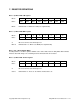
2. I/O HEADER PINOUT Ruby-MM-1612 provides a 50-pin right-angle header labeled J3 for all user I/O. This header is located on the right side of the board. Pins 1, 2, 49, and 50 are marked to aid in proper orientation. A standard 50-pin cable-mount IDC (insulation displacement contact) connector will mate with this header.
3. BOARD CONFIGURATION Refer to the Drawing of Ruby-MM-1612 on Page 8 for locations of headers described in Chapters 3 and 4. Base Address Each board in the system must have a different base address. Use the pin header labeled J5, base address. The numbers above the jumpers correspond to the I/O address bits; bit 9 is the MSB and bit 0 is the LSB. Only bits 9 – 4 are used for the base address decoding. The remaining 4 bits 3-0 are assumed to be 0 for the base address.
4. ANALOG OUTPUT RANGE CONFIGURATION Refer to the Drawing of Ruby-MM-1612 on Page 8 for locations of headers described in Sections 3 and 4. Refer to Figure 4.1 on Page for an explanation of the voltage reference circuitry. Also refer to Table 4.1 for a quick guide to output range configuration and jumper settings. Header J4 is used to configure the analog outputs.
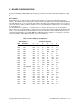
Table 4.1: Analog Output Configuration (Header J4) Range 5 F 0-5V: 0-10V: +/-5V: +/-10V: 0-2.5V: or +/-2.5V: or X X X X X X X X A B U X X X X X X X X X X X X An X means that a jumper is installed in that location. Only one half of pin header J4 is shown. Positions F A B U are repeated for each bank of 8 channels. ⇒ Note: Each bank of eight channels (0 - 7 and 8 - 15) can have a different output range setting. However, all eight channels within a bank will always have the same output range.
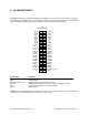
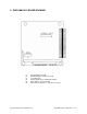
5. RUBY-MM-1612 BOARD DRAWING J1: J2: J3: J4: J5: J6: PC/104 8-bit bus header PC/104 16-bit bus header (not used) User I/O header Analog output range configuration header Base address selection header ISP header for factory use only; do not connect Copyright 2001 Diamond Systems Corp. Ruby-MM-1612 User Manual V1.1 P.
6. I/O MAP Ruby-MM-1612 occupies 8 consecutive 8-bit locations in I/O space. For example, the default base address is 300 Hex (768 Decimal); in this case the board occupies addresses 300 - 307 (768 - 775). The first 2 locations are used individually for each analog output channel. Since analog output data is 12 bits wide, it is broken into two bytes.
7. REGISTER DEFINITIONS Base + 0, Write: DAC LSB register Bit No. 7 6 5 4 3 2 1 0 Name DA7 DA6 DA5 DA4 DA3 DA2 DA1 DA0 DA7-0 D/A data bits 7-0. DA0 is the LSB (least significant bit). Base + 1, Write: DAC MSB register Bit No. 7 6 5 4 3 2 1 0 Name X X X X DA11 DA10 DA9 DA8 X Bit not used. These bits will be ignored. DA11-8 D/A data bits 11-8. DA11 is the MSB (most significant bit).
Base + 3, Write: External trigger register Bit No. 7 6 5 4 3 2 1 0 Name X X X X X X X TRIGEN X Bit not used. These bits will be ignored. TRIGEN External trigger enable. 1 = enable, 0 = disable. When external trigger is enabled, digital I/O line C0 will update all DACs simultaneously when it is brought low. This can be done either by an external signal, when C0 is in input mode, or in software, when C0 is in output mode.
8. 82C55 DIGITAL I/O CHIP OPERATION This is a short form description of the 82C55 digital I/O chip on the board. A full datasheet is included at the back of this manual.
9. ANALOG OUTPUT RANGES AND RESOLUTION The table below lists the available fixed full-scale output ranges and their corresponding actual full-scale voltage ranges and resolution. For any output range, the resolution is equal to the maximum possible range of output voltages divided by the maximum number of possible steps.
10. D/A CODE COMPUTATION Two different methods are used to compute the 12-bit D/A code used for analog output operations. For unipolar output ranges (positive voltages only), straight binary coding is used. For bipolar output ranges (both positive and negative voltages), offset binary coding is used. For any output range, the resolution is equal to the maximum possible range of output voltages divided by the maximum number of possible steps.
Offset Binary Coding (for bipolar output ranges) This method takes into account the fact that the lowest output voltage is not zero but a negative value. The output voltage is given by: Output Voltage = (Output Code / 2048) x Full-Scale Voltage - Full-Scale Voltage Example: Output code = 1024, full-scale voltage = 5V Output voltage = (1024 / 2048) x 5 - 5 = (0.5 x 5) - 5 = -2.
11. HOW TO GENERATE AN ANALOG OUTPUT This chapter describes how to generate an analog output directly (without the use of the driver software). Ruby-MM-1612 has 12-bit resolution analog outputs. However, data is written to the board in 8-bit bytes. Therefore two bytes must be written to the board to generate a single analog output. In addition, many applications require several channels to be updated simultaneously.
Examples Single channel output Assume channels 0 - 7 are configured for 0-5V. To set channel 0 to 3V, do the following: D/A code is 3V / 5V x 4096 = 2458 (value is rounded to nearest integer) LSB = 2458 AND 255 = 154 MSB = (2458 AND 3840) / 256 = 9 Step 1. Write 154 to base + 0 (LSB register). Step 2. Write 0 to base + 2 (Channel register). Step 3. Write 9 to base + 1 (MSB register). The value 2458 is written to DAC 0. Step 4. Read from base + 0. DAC 0 now outputs 3.000V.
12. CALIBRATION PROCEDURE Calibration requires a voltmeter (at least 5 digits of precision is preferred) and a miniature screwdriver to turn the potentiometer screws. The common lead of the voltmeter must be connected to analog ground (not digital ground). The best source for this connection is any of the analog ground pins on the user I/O header J3. ⇒ Note: All steps should be completed in the sequence shown, since each step affects the following steps.
13. SPECIFICATIONS Analog Outputs No. of outputs 16 voltage outputs Resolution 12 bits (1 part in 4096) Fixed output ranges 0 - 5V, 0 - 10V unipolar, ±5V, ±10V bipolar Adjustable output range Preset to 2.5V for 0 - 2.5V, ±2.5V output ranges Can be adjusted anywhere between approx. 1V and 2.5V External reference 0V min, 10V max Settling time 6µs max to ±.
82C55A CMOS Programmable Peripheral Interface June 1998 Features Description • Pin Compatible with NMOS 8255A The Intersil 82C55A is a high performance CMOS version of the industry standard 8255A and is manufactured using a self-aligned silicon gate CMOS process (Scaled SAJI IV). It is a general purpose programmable I/O device which may be used with many different microprocessors. There are 24 I/O pins which may be individually programmed in 2 groups of 12 and used in 3 major modes of operation.
82C55A Pin Description SYMBOL PIN NUMBER VCC 26 VCC: The +5V power supply pin. A 0.1µF capacitor between pins 26 and 7 is recommended for decoupling. GND 7 GROUND D0-D7 27-34 I/O RESET 35 I RESET: A high on this input clears the control register and all ports (A, B, C) are set to the input mode with the “Bus Hold” circuitry turned on. CS 6 I CHIP SELECT: Chip select is an active low input used to enable the 82C55A onto the Data Bus for CPU communications.
82C55A Functional Description POWER SUPPLIES Data Bus Buffer This three-state bi-directional 8-bit buffer is used to interface the 82C55A to the system data bus. Data is transmitted or received by the buffer upon execution of input or output instructions by the CPU. Control words and status information are also transferred through the data bus buffer.
82C55A register will contain 9Bh. During the execution of the system program, any of the other modes may be selected using a single output instruction. This allows a single 82C55A to service a variety of peripheral devices with a simple software maintenance routine. Any port programmed as an output port is initialized to all zeros when the control word is written. Ports A, B, and C The 82C55A contains three 8-bit ports (A, B, and C).
82C55A The modes for Port A and Port B can be separately defined, while Port C is divided into two portions as required by the Port A and Port B definitions. All of the output registers, including the status flip-flops, will be reset whenever the mode is changed. Modes may be combined so that their functional definition can be “tailored” to almost any I/O structure.
82C55A Mode 0 (Basic Input) tRR RD tIR tHR INPUT tAR tRA CS, A1, A0 D7-D0 tRD tDF Mode 0 (Basic Output) tWW WR tWD tDW D7-D0 tAW tWA CS, A1, A0 OUTPUT tWB Mode 0 Configurations CONTROL WORD #0 CONTROL WORD #2 D7 D6 D5 D4 D3 D2 D1 D0 1 0 0 0 0 0 0 D7 D6 D5 D4 D3 D2 D1 D0 0 1 8 A 82C55A 4 4 8 B 0 0 0 0 1 0 82C55A 4 PC7 - PC4 PA7 - PA0 PC7 - PC4 C D7 - D0 4 PC3 - PC0 8 PB7 - PB0 B PC3 - PC0 PB7 - PB0 CONTROL WORD #3 0 0 D7 D6 D5 D4 D3 D2 D1 D0 1 1 8 A 82C55
82C55A Mode 0 Configurations (Continued) CONTROL WORD #4 CONTROL WORD #8 D7 D6 D5 D4 D3 D2 D1 D0 1 0 0 0 1 0 0 D7 D6 D5 D4 D3 D2 D1 D0 0 1 8 A 82C55A 4 4 8 B 0 0 1 0 0 82C55A 4 8 8 B 0 1 82C55A PB7 - PB0 0 0 0 1 82C55A 4 PC7 - PC4 PA7 - PA0 PC7 - PC4 C D7 - D0 4 PC3 - PC0 8 PB7 - PB0 B PC3 - PC0 PB7 - PB0 D7 D6 D5 D4 D3 D2 D1 D0 1 4 4 8 B 0 0 1 0 0 1 0 8 PA7 - PA0 A 82C55A 4 PC7 - PC4 PA7 - PA0 PC7 - PC4 C D7 - D0 4 PC3 - PC0 8 PB7 - PB0
82C55A Mode 0 Configurations (Continued) CONTROL WORD #12 CONTROL WORD #14 D7 D6 D5 D4 D3 D2 D1 D0 1 0 0 1 1 0 0 D7 D6 D5 D4 D3 D2 D1 D0 0 1 8 A 82C55A 4 4 8 B 0 1 1 1 0 1 0 8 82C55A PA7 - PA0 4 PC7 - PC4 PC7 - PC4 C D7 - D0 4 PC3 - PC0 PC3 - PC0 8 PB7 - PB0 PB7 - PB0 B CONTROL WORD #15 D7 D6 D5 D4 D3 D2 D1 D0 0 1 A CONTROL WORD #13 1 0 PA7 - PA0 C D7 - D0 0 0 0 D7 D6 D5 D4 D3 D2 D1 D0 1 1 8 A 82C55A D7 - D0 4 8 B 0 1 1 0 1 1 8 PA7 - PA0 PA7
82C55A tST STB tSIB IBF tSIT tRIB INTR tRIT RD tPH INPUT FROM PERIPHERAL tPS FIGURE 7. MODE 1 (STROBED INPUT) INTR (Interrupt Request) INTE A A “high” on this output can be used to interrupt the CPU when and input device is requesting service. INTR is set by the condition: STB is a “one”, IBF is a “one” and INTE is a “one”. It is reset by the falling edge of RD. This procedure allows an input device to request service from the CPU by simply strobing its data into the port.
82C55A tWOB WR tAOB OBF INTR tWIT ACK tAK tAIT OUTPUT tWB FIGURE 9.
82C55A CONTROL WORD D7 D6 D5 D4 D3 D2 D1 D0 1 1 INTRA PC3 1/0 1/0 1/0 PA7-PA0 PC2-PC0 1 = INPUT 0 = OUTPUT PORT B 1 = INPUT 0 = OUTPUT 8 PC7 OBFA INTE 1 PC6 ACKA INTE 2 PC4 STBA PC5 IBFA WR GROUP B MODE 0 = MODE 0 1 = MODE 1 PC2-PC0 RD FIGURE 11. MODE CONTROL WORD 3 I/O FIGURE 12.
82C55A MODE 2 AND MODE 0 (INPUT) MODE 2 AND MODE 0 (OUTPUT) PC3 PA7-PA0 1 1 0 1 1/0 PC2-PC0 1 = INPUT 0 = OUTPUT PA7-PA0 8 OBFA PC7 CONTROL WORD D7 D6 D5 D4 D3 D2 D1 D0 PC6 ACKA PC4 STBA PC5 IBFA PC2-PC0 PC3 INTRA 3 CONTROL WORD D7 D6 D5 D4 D3 D2 D1 D0 1 1 0 ACKA PC4 STBA IBFA PC5 3 I/O 8 WR MODE 2 AND MODE 1 (INPUT) PC3 PA7-PA0 CONTROL WORD D7 D6 D5 D4 D3 D2 D1 D0 0 PA7-PA0 8 OBFA PC6 ACKA PC4 STBA PC5 IBFA PC1 PC3 INTRA PC7 PB7-PB0 WR PC6 PB7, PB0 8 MODE 2
82C55A MODE DEFINITION SUMMARY MODE 1 MODE 0 MODE 2 IN OUT IN OUT PA0 PA1 PA2 PA3 PA4 PA5 PA6 PA7 In In In In In In In In Out Out Out Out Out Out Out Out In In In In In In In In Out Out Out Out Out Out Out Out PB0 PB1 PB2 PB3 PB4 PB5 PB6 PB7 In In In In In In In In Out Out Out Out Out Out Out Out In In In In In In In In Out Out Out Out Out Out Out Out PC0 PC1 PC2 PC3 PC4 PC5 PC6 PC7 In In In In In In In In Out Out Out Out Out Out Out Out INTRB IBFB STBB INTRA STBA IBFA I/O I/O INTRB OBF
82C55A Reading Port C Status (Figures 15 and 16) Applications of the 82C55A In Mode 0, Port C transfers data to or from the peripheral device. When the 82C55A is programmed to function in Modes 1 or 2, Port C generates or accepts “hand shaking” signals with the peripheral device. Reading the contents of Port C allows the programmer to test or verify the “status” of each peripheral device and change the program flow accordingly.