
User's Manual
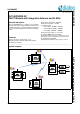
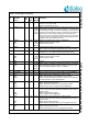
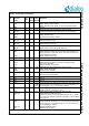
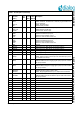
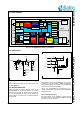
Table Of Contents
- 1.0 Connection diagram
- 2.0 Introduction
- 3.0 Specifications
- 3.1 GENERAL
- 3.2 ABSOLUTE MAXIMUM RATINGS
- 3.3 Operating Conditions
- 3.4 Digital Input/Output Pins
- 3.5 ULTRA LOW ENERGY (ULE) I/O PIN
- 3.6 SUPPLY CURRENTS
- 3.7 Analog Front End
- Table 10: Microphone amplifier
- Table 11: Microphone amplifier (Operating Condition)
- Table 12: Microphone supply voltages
- Table 13: VREFp load circuit
- Table 14: LSRp/LSRn outputs
- Table 15: LSRp/LSRn load circuits
- Table 16: PAOUTp, PAOUTn outputs
- Table 17: PAOUTp, PAOUTn outputs (Note 21)
- Table 18: PAOUTp, PAOUTn external components
- 3.8 Battery management
- 3.9 Baseband Part
- 3.10 Radio (RF) Part
- 3.11 RF Power supply
- 3.12 RF channel frequencies
- 4.0 Design guidelines
- 5.0 Notices to OEM
- 6.0 Package information
- 7.0 Revision history

SC14SPNODE SF DECT Module with integrated Antenna and FLASH
© 2012 Dialog Semiconductor B.V. 8 Jul 1, 2014 v1.6
Note 1: “NC” means: leave unconnected.
“GND” means internally connected to the module ground plane. Every GND pin should be connected to the main PCB.ground plane.
Note 2: All digital inputs have Schmitt trigger inputs. After reset all I/Os are set to input and all pull-up or pull-down resistors are enabled unless oth-
erwise specified.
PU = Pull-up resistor enabled, PD = Pull-down resistor enabled, I = input,
O = output, Hi-Z = high impedance, 1 = logic HIGH level, 0 = logic LOW level
Refer also to Px_DIR_REGs for INPUT/OUTPUT and Pull-up/Pull-down configurations
Note 3: Back drive protected pins allow always interfacing with devices up to a supply voltage of 3.45 V.
If PAD_CTRL_REG[xxx_OD] bit is set then
1) the internal Pull-up resistors are always disabled to prevent currents from 1.8 V < Vin < 3.45 V to VDD.
2) If port is set to output, the output is always configured as open drain to allow the output level to reach Vin >1.8 V. The external pull-up
resistor value determines the rise time of the signal.
Note 4: For base station applications with high line input voltages, an input protection on all ADC inputs can be enabled with
AD_CTRL_REG[ADCx_PR_DIS] =’0’. To limit the input current as specified in chapter “specifications”, an external resistor must placed in
series with the ADC inputs. With the input protection enabled, the ADC is linear from 0 to 0.9 V. With ADCx_PR_DIS=’1’ the ADC0 and
ADC1 are linear from 0 V to 1.8 V.
Note 5: In digital mode extra static VDDPA current will flow (See Supply currents (indicative value) (table 9, page 14)). So the digital mode is not
recommended in portable applications.The reason for this output overvoltage protection is that a speaker is an inductor (which can store
energy). In case the battery is removed from the handset while handsfree speaker is active, the battery voltage could become too high
when the inductor releases its energy to the battery (which is not present anymore as a buffer). To prevent this electrical overstress situa-
tion, the overvoltage protection is added.
Note 6: This pin description describes all function that is supported by hardware. Supported pin function depends on installed software.
Note 7: All ULP pins use snap-back devices as ESD protection, which (when triggered) have a holding voltage below the typical battery voltage.
This means that the snap-back device of a ULP pin may remain conductive, when triggered while the pin is directly connected to the battery
voltage. If any of the ULP pins are directly or indirectly electrically accessible on the outside of the application, system level ESD precau-
tions must be taken to ensure that the snap-back device is not triggered while in active mode, to prevent the chip from being damaged.
81-88 TP2 to TP9 NC Must be left unconnected. See section 4.1 and Figure 15.
Table 1: Pin description (Continued)
Pin
Module
Pin name
(Note 1)
In/
Out
Iout
Drive
(mA)
Reset
State
(Note 2)
Description