
User's Manual
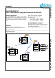
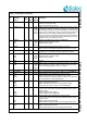
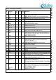
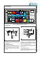
Table Of Contents
- 1.0 Connection diagram
- 2.0 Introduction
- 3.0 Specifications
- 3.1 GENERAL
- 3.2 ABSOLUTE MAXIMUM RATINGS
- 3.3 Operating Conditions
- 3.4 Digital Input/Output Pins
- 3.5 ULTRA LOW ENERGY (ULE) I/O PIN
- 3.6 SUPPLY CURRENTS
- 3.7 Analog Front End
- Table 10: Microphone amplifier
- Table 11: Microphone amplifier (Operating Condition)
- Table 12: Microphone supply voltages
- Table 13: VREFp load circuit
- Table 14: LSRp/LSRn outputs
- Table 15: LSRp/LSRn load circuits
- Table 16: PAOUTp, PAOUTn outputs
- Table 17: PAOUTp, PAOUTn outputs (Note 21)
- Table 18: PAOUTp, PAOUTn external components
- 3.8 Battery management
- 3.9 Baseband Part
- 3.10 Radio (RF) Part
- 3.11 RF Power supply
- 3.12 RF channel frequencies
- 4.0 Design guidelines
- 5.0 Notices to OEM
- 6.0 Package information
- 7.0 Revision history

SC14SPNODE SF DECT Module with integrated Antenna and FLASH
© 2012 Dialog Semiconductor B.V. 6 Jul 1, 2014 v1.6
37 P1[1]/
INT1/
LE
IO 2 I-PU INPUT/OUTPUT with selectable pull up/down resistor.
INPUT. Keyboard input interrupt.
INPUT. MicroWire latch enable. (for monitoring/external radio).
38 GND - - - Ground
39 P2[6]/
WTF_IN
IO 2 I-PU INPUT/OUTPUT with selectable pull up/down resistor.
OUTPUT. Gen2DSP enable signal used to monitor DSP load
40 P0[7]/
SPI_DI/
PWM1
IO 8 I-PU INPUT/OUTPUT with selectable pull up/down resistor.
INPUT. SPI data input.
OUTPUT. Timer 0 PWM 1 output.
41 P0[6]/
SPI_DO
IO 8 I-PU INPUT/OUTPUT with selectable pull up/down resistor.
OUTPUT. SPI data output.
42 P0[5]/
SPI_CLK
IO 8 I-PU INPUT/OUTPUT with selectable pull up/down resistor.
INPUT/OUTPUT. SPI clock.
43 P0[4]/
SPI_EN
IO 8 I-PU INPUT/OUTPUT with selectable pull up/down resistor.
INPUT/OUTPUT. SPI clock enable. Active low.
44 P0[3]/
SCL2/
URX2
IO 8 I-PU INPUT/OUTPUT with selectable pull up/down resistor.
INPUT/OUTPUT. ACCESS bus 2 clock with programmable Push-
pull or open drain. In open drain mode, SCL2 is monitored to sup-
port bit stretching by a slave.
INPUT. UART2 receive data
45 GND - - - Ground
46 P0[2]/
SDA2/
UTX2
IO 8 I-PU INPUT/OUTPUT with selectable pull up/down resistor.
INPUT/OUTPUT. ACCESS bus 2 data with programmable.
Push-pull or open drain.
OUTPUT. UART2 transmit data
47 P0[1]/
URX/
PWM0
IO 8 I-PD
(10k)
INPUT/OUTPUT with selectable pull up/down resistor.
INPUT. UART receive data.
OUTPUT. Timer 0 PWM0
48 P0[0]/
UTX
O 8 I-PU INPUT/OUTPUT with selectable pull up/down resistor.
OUTPUT. UART transmit data.
49 GND - - - Ground
50 GND - - - Ground
51 GND - - - Ground
52 RSTn I 1 I-PU
(200k
pull-up)
Active low Reset input with Schmitt-trigger input, open-drain output
and pull up resistor to internal VDD. Input may not exceed 2.0 V. An
internal capacitor of 47 nF is mounted on this pin.
53 JTAG IO 8 I-PU JTAG-SDI+; one wire Debug interface with open-drain.
Requires external 1 k Pull-up to VDD.
54 P2[5]/
PCM_FSC/
SF
IO 8 I-PU INPUT/OUTPUT with selectable pull up/down resistor.
INPUT/OUTPUT. PCM Frame Sync.
OUTPUT. S-field Sync found signal indicating the 00 or 11 pream-
ble to unique word transition with 96 ns resolution. Used for debug-
ging purposes.
55 P2[4]/
SCL1/
PCM_DO/
DP3
IO 8 I-PU INPUT/OUTPUT with selectable pull up/down resistor.
INPUT / OUTPUT. ACCESS bus 1 clock with programmable Push-
pull or open drain. In open drain mode, SCL1 is monitored to sup-
port bit stretching by a slave.
OUTPUT. PCM data output.
OUTPUT. DIP port DP3.
Table 1: Pin description (Continued)
Pin
Module
Pin name
(Note 1)
In/
Out
Iout
Drive
(mA)
Reset
State
(Note 2)
Description