
User's Manual
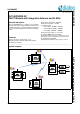
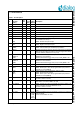
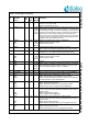
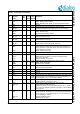
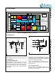
Table Of Contents
- 1.0 Connection diagram
- 2.0 Introduction
- 3.0 Specifications
- 3.1 GENERAL
- 3.2 ABSOLUTE MAXIMUM RATINGS
- 3.3 Operating Conditions
- 3.4 Digital Input/Output Pins
- 3.5 ULTRA LOW ENERGY (ULE) I/O PIN
- 3.6 SUPPLY CURRENTS
- 3.7 Analog Front End
- Table 10: Microphone amplifier
- Table 11: Microphone amplifier (Operating Condition)
- Table 12: Microphone supply voltages
- Table 13: VREFp load circuit
- Table 14: LSRp/LSRn outputs
- Table 15: LSRp/LSRn load circuits
- Table 16: PAOUTp, PAOUTn outputs
- Table 17: PAOUTp, PAOUTn outputs (Note 21)
- Table 18: PAOUTp, PAOUTn external components
- 3.8 Battery management
- 3.9 Baseband Part
- 3.10 Radio (RF) Part
- 3.11 RF Power supply
- 3.12 RF channel frequencies
- 4.0 Design guidelines
- 5.0 Notices to OEM
- 6.0 Package information
- 7.0 Revision history

SC14SPNODE SF DECT Module with integrated Antenna and FLASH
© 2012 Dialog Semiconductor B.V. 4 Jul 1, 2014 v1.6
1.1 PIN DESCRIPTION
Table 1: Pin description
Pin
Module
Pin name
(Note 1)
In/
Out
Iout
Drive
(mA)
Reset
State
(Note 2)
Description
1 GND - - - Ground
2 P0 O 8 Hi-Z Control port for FAD. See 2.6
3 RFP0 O 8 Hi-Z Control port for FAD. See 2.6
4 P0n O 8 Hi-Z Control port for FAD. See 2.6
5 RFP0n O 8 Hi-Z Control port for FAD. See 2.6
6 GND - - - Ground
7 VREFp O - I Positive microphone supply voltage
8CIDINn
MICp
I - I INPUT. Caller-id opamp negative input with switchable input protec-
tion enabled from start-up.
INPUT. Positive microphone input.
9CIDOUT/
MICn
IO - I OUTPUT. Caller-id opamp output to ADC.
INPUT. Negative microphone input.
10 MICh/
LINEIN
I - I INPUT. Headset microphone input with fixed input protection
INPUT. Line interface input with fixed input protection
11 VREFm - - - Negative microphone reference. This pin must also be connected to
GND ground, but make sure that the microphone ground is directly
routed to VREFm (VREFm is the star point).
12 LSRp/
LINEOUT/
AGND
O - O OUTPUT. Positive loudspeaker output
OUTPUT. To Line interface.
OUTPUT. Buffered analog ground (0.9 V) if LSRP_MODE = 00.
13 LSRn/
LINEOUT/
AGND
O - O OUTPUT. Negative loudspeaker output.
OUTPUT. To Line interface.
OUTPUT. Buffered analog ground (0.9 V) if LSRN_MODE = 00.
14 GND - - - Ground
15 P3[3]/
ADC0
IO 8 I INPUT/OUTPUT with selectable pull up/down resistor.
INPUT. ADC0 input to ADC with programmable input protection
enabled from reset. (Note 4)
16 P1[0]/
INT0/
ADC1
IO 2 I-PU INPUT/OUTPUT with selectable pull up/down resistor.
INPUT. Keyboard input interrupt.
INPUT. ADC1 input to ADC with programmable input protection
enabled from reset. (Note 4)
17 SOCp I - I Battery State Of Charge positive input.
Connect to GND if not used.
18 SOCn I - I Battery State Of Charge negative input. Star point connected to the
SOC resistor. Connect to GND if not used.
19 DC_SENCE I I INPUT. Voltage sense input. Connected via a resistor divider to the
output of the DC/C converter. Maximum 1.27 V
Connect to GND if not used.
20 DC_I I I Current sense input of DC/DC converter. Connect to GND if not
used
21 DC_CTRL O 2 O-PD
(fixed
100k
pull-
down)
OUTPUT. Switching clock for the DC/DC converter, this pad is sup-
plied with VBAT.
Leave unconnected if not used.