
User's Manual
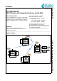
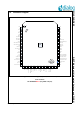
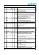
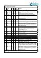
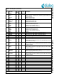
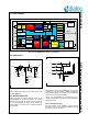
Table Of Contents
- 1.0 Connection diagram
- 2.0 Introduction
- 3.0 Specifications
- 3.1 GENERAL
- 3.2 ABSOLUTE MAXIMUM RATINGS
- 3.3 Operating Conditions
- 3.4 Digital Input/Output Pins
- 3.5 ULTRA LOW ENERGY (ULE) I/O PIN
- 3.6 SUPPLY CURRENTS
- 3.7 Analog Front End
- Table 10: Microphone amplifier
- Table 11: Microphone amplifier (Operating Condition)
- Table 12: Microphone supply voltages
- Table 13: VREFp load circuit
- Table 14: LSRp/LSRn outputs
- Table 15: LSRp/LSRn load circuits
- Table 16: PAOUTp, PAOUTn outputs
- Table 17: PAOUTp, PAOUTn outputs (Note 21)
- Table 18: PAOUTp, PAOUTn external components
- 3.8 Battery management
- 3.9 Baseband Part
- 3.10 Radio (RF) Part
- 3.11 RF Power supply
- 3.12 RF channel frequencies
- 4.0 Design guidelines
- 5.0 Notices to OEM
- 6.0 Package information
- 7.0 Revision history

SC14SPNODE SF DECT Module with integrated Antenna and FLASH
© 2012 Dialog Semiconductor B.V. 3 Jul 1, 2014 v1.6
1.0 Connection diagram
Figure 1 Connection diagram (top view, leads face down)
Order numbers:
SC14SPNODE SF01T (tray, MPQ = 600 pcs)
1
23
22
21
20
19
18
17
16
15
14
13
12
11
10
9
8
7
6
5
4
3
2
27
49
48
47
46
45
44
43
42
41
40
39
38
37
36
35
34
33
32
31
30
29
28
26
25
24
72
50
51
52
53
54
55
56
57
58
59
60
61
62
63
64
65
66
67
68
69
70
71
79
80
GND
PARADET/P3[4]
P2[0]/ECZ1/PWM0/LED3
GND
TP1
RINGOUT/RINGING/P3[5]
GND
RFP0
P0
GND
GND
ADC0/P3[3]
LSRn/LINEOUT/AGND
LSRp/LINEOUT/AGND
VREFm
MICn/CIDOUT
MICp/CIDINn
VREFp
MICh/LINEIN
CIDINp/P3[2]
RINGp/P3[7]
RINGn/P3[6]
DC_I
DC_SENSE
SOCn
SOCp
ADC1/INT0/P1[0]
DC_CTRL
VDDE/RDI/INT5/P1[5]
ULP_PORT
ULP_XTAL
PON/P1[6]
CP_VOUT1
GND
DP0/PAOUTn/P3[0]
VDDPA
DP1/PAOUTp/P3[1]
CHARGE/P1[7]
CHARGE_CTRL
VBATSW
VBATIN
VBATIN
VDDOUT
GND
SIO/INT3/P1[3]
TDOD/INT4/P1[4]
BXTAL/INT7/P2[7]
SK/INT2/P1[2]
LE/INT1/P1[1]
P0[7]/PWM1SPI_DI
P0[6]/SPI_DO
GND
WTF_IN/P2[6]
P0[4]/SPI_EN
P0[3]/SCL2/URX2
P0[5]/SPI_CLK
P0[2]/SDA2/UTX2
P0[1]/PWM0/URX
P0[0]/UTX
GND
RSTn
JTAG
SF/P2[5]/PCM_FSC
DP3/P2[4]/SCL1/PCM_DO
DP2/P2[3]/SDA1/PCM_DI
CLK100/P2[2]/PCM_CLK
P2[1]/ECZ2/PWM1/LED4
RFP0n
P0n
RF1
GND
RF0
GND
GND
GND
GND
GND
78
77
76
75
74
73
GND
GND
GND
81
82
83
84
87
88
85
86