
User's Manual
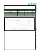
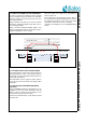
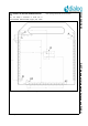
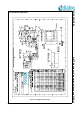
Table Of Contents
- 1.0 Connection diagram
- 2.0 Introduction
- 3.0 Specifications
- 3.1 GENERAL
- 3.2 ABSOLUTE MAXIMUM RATINGS
- 3.3 Operating Conditions
- 3.4 Digital Input/Output Pins
- 3.5 ULTRA LOW ENERGY (ULE) I/O PIN
- 3.6 SUPPLY CURRENTS
- 3.7 Analog Front End
- Table 10: Microphone amplifier
- Table 11: Microphone amplifier (Operating Condition)
- Table 12: Microphone supply voltages
- Table 13: VREFp load circuit
- Table 14: LSRp/LSRn outputs
- Table 15: LSRp/LSRn load circuits
- Table 16: PAOUTp, PAOUTn outputs
- Table 17: PAOUTp, PAOUTn outputs (Note 21)
- Table 18: PAOUTp, PAOUTn external components
- 3.8 Battery management
- 3.9 Baseband Part
- 3.10 Radio (RF) Part
- 3.11 RF Power supply
- 3.12 RF channel frequencies
- 4.0 Design guidelines
- 5.0 Notices to OEM
- 6.0 Package information
- 7.0 Revision history

SC14SPNODE SF DECT Module with integrated Antenna and FLASH
© 2012 Dialog Semiconductor B.V. 24 Jul 1, 2014 v1.6
4.2 MODULE PLACEMENT ON THE MAIN BOARD
In order to ensure FCC compliance, proper coverage
and to avoid detuning of the antennas, it is required to
place the module on the main board free from other
surrounding materials.
Keep a distance of at least 10 mm from the antenna
elements to conducting objects and at least 5 mm to
non-conducting objects.
Keep in mind that electrical shielding objects, even
partly surrounding the antennas, will normally cause a
significant degradation of the coverage.
Place the module at the edge of the main-board as
shown in Figure 16.
If the module has to be placed away from the edge of
the main-board, then avoid conducting areas in front of
the antennas and make a cut-out in the main board
underneath the antennas as shown in the figure.
See Figure 18 and Figure 21 for the detailed package
outline.
4.3 PATTERN FOR PIN 79 ON THE MAIN BOARD
The copper pattern for pin 79 on the main board is very
important because it is part of the internal antenna of
the module. It is used to extend the internal antenna for
optimum RF performance.
The PCB pattern shown in Figure 19 under “pads C”
for pin 79 on the main board was used during module
certification.
4.4 PRECAUTIONS REGARDING UNINTENDED
COUPLING
The SC14SPNODE includes an internal antenna, so by
integration on the main board precautions shall be
taken in order to avoid any kind of coupling from the
main board to the RF part of the module.
If there is any doubt about this, a brief radio test should
be performed.
Figure 16 Module placement on the main board (top view)
1 78
No PCB area
2
3 76
77
GND
GND GND
79
Main boardModule
antenna extension
> 10 mm
> 10 mm
> 10 mm