
User's Manual
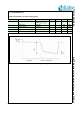
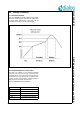
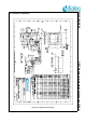
Table Of Contents
- 1.0 Connection diagram
- 2.0 Introduction
- 3.0 Specifications
- 3.1 GENERAL
- 3.2 ABSOLUTE MAXIMUM RATINGS
- 3.3 Operating Conditions
- 3.4 Digital Input/Output Pins
- 3.5 ULTRA LOW ENERGY (ULE) I/O PIN
- 3.6 SUPPLY CURRENTS
- 3.7 Analog Front End
- Table 10: Microphone amplifier
- Table 11: Microphone amplifier (Operating Condition)
- Table 12: Microphone supply voltages
- Table 13: VREFp load circuit
- Table 14: LSRp/LSRn outputs
- Table 15: LSRp/LSRn load circuits
- Table 16: PAOUTp, PAOUTn outputs
- Table 17: PAOUTp, PAOUTn outputs (Note 21)
- Table 18: PAOUTp, PAOUTn external components
- 3.8 Battery management
- 3.9 Baseband Part
- 3.10 Radio (RF) Part
- 3.11 RF Power supply
- 3.12 RF channel frequencies
- 4.0 Design guidelines
- 5.0 Notices to OEM
- 6.0 Package information
- 7.0 Revision history

SC14SPNODE SF DECT Module with integrated Antenna and FLASH
© 2012 Dialog Semiconductor B.V. 21 Jul 1, 2014 v1.6
3.11 RF POWER SUPPLY
Table 24: Requirements for linear supply regulator
PARAMETER DESCRIPTION CONDITIONS MIN TYP MAX UNIT
VBAT IN Voltage at VBAT SW Unloaded V
B
Loaded V
B
-V
1
-V
2
-V
3
2.1 3 3.45 V
V
1
Settling time I = 50 mA 20 mV
V
2
Receive period I = 130 mA 100 mV
V
2
Transmit period I = 550 mA 200 mV
V
3
Drop during transmit 25 mV
Figure 14 RF power supply
B