
User's Manual
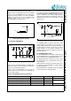
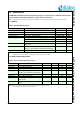
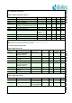
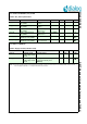
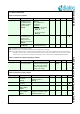
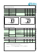
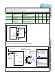
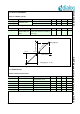
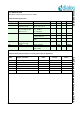
Table Of Contents
- 1.0 Connection diagram
- 2.0 Introduction
- 3.0 Specifications
- 3.1 GENERAL
- 3.2 ABSOLUTE MAXIMUM RATINGS
- 3.3 Operating Conditions
- 3.4 Digital Input/Output Pins
- 3.5 ULTRA LOW ENERGY (ULE) I/O PIN
- 3.6 SUPPLY CURRENTS
- 3.7 Analog Front End
- Table 10: Microphone amplifier
- Table 11: Microphone amplifier (Operating Condition)
- Table 12: Microphone supply voltages
- Table 13: VREFp load circuit
- Table 14: LSRp/LSRn outputs
- Table 15: LSRp/LSRn load circuits
- Table 16: PAOUTp, PAOUTn outputs
- Table 17: PAOUTp, PAOUTn outputs (Note 21)
- Table 18: PAOUTp, PAOUTn external components
- 3.8 Battery management
- 3.9 Baseband Part
- 3.10 Radio (RF) Part
- 3.11 RF Power supply
- 3.12 RF channel frequencies
- 4.0 Design guidelines
- 5.0 Notices to OEM
- 6.0 Package information
- 7.0 Revision history

SC14SPNODE SF DECT Module with integrated Antenna and FLASH
© 2012 Dialog Semiconductor B.V. 11 Jul 1, 2014 v1.6
2.6.2 Internal and external antenna with FAD
Figure 5 shows one external antenna that is connected
to RF1 of the SC14SPNODE SF. This configuration
supports the FAD function. In this case pins RFP0,
RFP0n, P0 and P0n must be left unconnected. The
software patch code is not needed if the
SC14SPNODE SF is operated as FP.
2.7 BATTERY MANAGEMENT
Figure 6 shows a handset application with NiMH. SOC
(State Of Charge) is used to measure the amount of
charge in the rechargeable batteries.
Figure 7 shows an FP application. The FP uses an
external LDO, so the SOC pins are not used and can
be connected to GND.
The SOC circuit is used to very accurately determine
the amount of charge in rechargeable batteries as well
as the discharge state of Alkaline batteries. This infor-
mation is essential for the battery charging algorithm
and necessary for battery status indication to the user.
Detailed information can be found in AN-D-174 (see
Reference [2]).
Pin CHARGE_CTRL is driven high when either
“sensed voltage on the VBAT pin” is lower than the
voltage setting (defined by the module hardware) or
“sensed current via SOCp” is lower than the current
setting (defined by the module hardware). Pin
CHARGE_CTRL can drive up to 500 A as source cur-
rent (see Table 19).
2.8 EMBEDDED QSPI FLASH
The SC14SPNODE SF has a QSPI FLASH with type
number MX25U1635E as embedded FLASH. Please
refer to Reference [3] for detailed specifications.
The MX25U1635E has an OTP area, a part of which
has already been factory programmed by Dialog for
tuning purposes.
Table 2 shows the production parameters and the rela-
tion between the SC14SPNODE SF register address
and the OTP address.
The OTP addresses from 0x020 to 0x1FF are available
for write access before locking the OTP.
Figure 5 One external antenna
Figure 6 Handset (PP) application with 2x NiMH
External
Antenna
RF1
100
CHARGE_CTRL
1k
1k
0.1
SOC
CHARGE
SOCp
SOCn
Vsupply VBAT IN
SC14SPNODE
Figure 7 Base station (FP) application
CHARGE_CTRL
1k
SOC
CHARGE
SOCp
SOCn
Vsupply
VBAT IN
LDO
SC14SPNODE
Table 2: SC14SPNODE production parameters
Register name SC14SPNODE address OTP address Alignment Spec.
RF_BURST_MODE_CTRL_REG[MODINDEX] 0xFF7053[5:0] 0x05 340 kHz to 370 kHz
CLK_FREQ_TRIM_REG (lsb) 0xFF400A 0x06 20.736 MHz +/- 1 ppm
CLK_FREQ_TRIM_REG (msb) 0xFF400B 0x07
BANDGAP_REG 0xFF4810 0x08 1.8 V +/- 1%