
User's Manual
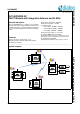
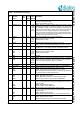
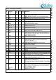
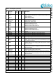
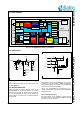
Table Of Contents
- 1.0 Connection diagram
- 2.0 Introduction
- 3.0 Specifications
- 3.1 GENERAL
- 3.2 ABSOLUTE MAXIMUM RATINGS
- 3.3 Operating Conditions
- 3.4 Digital Input/Output Pins
- 3.5 ULTRA LOW ENERGY (ULE) I/O PIN
- 3.6 SUPPLY CURRENTS
- 3.7 Analog Front End
- Table 10: Microphone amplifier
- Table 11: Microphone amplifier (Operating Condition)
- Table 12: Microphone supply voltages
- Table 13: VREFp load circuit
- Table 14: LSRp/LSRn outputs
- Table 15: LSRp/LSRn load circuits
- Table 16: PAOUTp, PAOUTn outputs
- Table 17: PAOUTp, PAOUTn outputs (Note 21)
- Table 18: PAOUTp, PAOUTn external components
- 3.8 Battery management
- 3.9 Baseband Part
- 3.10 Radio (RF) Part
- 3.11 RF Power supply
- 3.12 RF channel frequencies
- 4.0 Design guidelines
- 5.0 Notices to OEM
- 6.0 Package information
- 7.0 Revision history

SC14SPNODE SF DECT Module with integrated Antenna and FLASH
© 2012 Dialog Semiconductor B.V. 10 Jul 1, 2014 v1.6
2.4 BLOCK DIAGRAM
2.5 POWER SUPPLY
Figure 3 shows the internal power supply circuit of the
SC14SPNODE SF.
2.6 ANTENNA OPERATION
Figure 4 shows the internal antenna circuit of the
SC14SPNODE SF. Pin RF0 is used for two external
antennas and can also be used for RF test purposes,
so it is recommended to add a 10 pF capacitor as
reserve pattern even when the two external antennas
are not used.
Re-certification of the SC14SPNODE SF is required if
at least one external antenna is added. On request,
Dialog Semiconductor can provide a pre-certified PCB
layout for an external antenna circuit.
RF1 is also recommended to use and can be con-
nected to the RF cable to be able to do the JPN DECT
type approval test.
2.6.1 Internal antenna only
The FAD function is not enabled if only the internal
antenna is used. In this case RFP0, RFP0n, P0 and
P0n must be left unconnected.
Figure 2 SC14SPNODE hardware block diagram
Charge Pump
doubler
32kByte
Shared
RAM
JTAG
/SDI
CR16Cplus
(82.944 MHz)
Non Shared/
Cache/Trace
RAM 16+4kByte
QSPI
ULE
Cache
Controller
DCDC
DIP
DIP RAM
LDO
Class-D
PCM / I2S
AFE
8/16 kHz
CODEC
8/16 kHz
48/2 kByte
Gen2DSP
ROM/RAM
Gen2DSP
82 MIPS
DMA
UART
GPIO 0-3
10 bit ADC
2 x ACCESS
APB bridge
SPI
UART
PLL
(165.888
MHz)
XTAL
20.736
MHz
Radio
Transceiver
PA
TX/RX
SW
ANT
SW
16Mbit
FLASH
Power supply
GPIOs
SC14SPNODE
Figure 3 Internal circuit of the power supply
UPL_MAIN_CTRL
VBATIN
100n
100n
1U0
VBATSW
VDDOUT
VDD
VBAT
TX BALUN
RF_SUPPLY
RF_SUPPLY_PA
CP_BAT
ULP_BAT
ADD
Internal
FLASH VDD
LDO_CTRL
Figure 4 Internal circuit of the antenna part
RF1
TP1
Internal antenna
RF0
P0n
P0
TX
RX
RFP0n
RFP0