
User's Manual
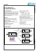
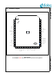
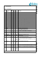
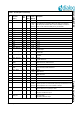
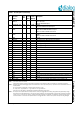
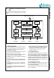
Table Of Contents
- 1.0 Connection diagram
- 2.0 Introduction
- 3.0 Cordless Voice Module functionality
- 4.0 Functional description
- 5.0 CAT-iq
- 6.0 Specifications
- 6.1 General
- 6.2 Absolute Maximum ratings
- 6.3 Operating Conditions
- 6.4 Digital Input/Output Pins
- 6.5 Analog Front End
- Table 11: Microphone amplifier
- Table 12: Microphone amplifier (Operating Condition)
- Table 13: Microphone supply voltages
- Table 14: VREFp load circuit
- Table 15: LSRp/LSRn outputs
- Table 16: LSRp/LSRn load circuits
- Table 17: PAOUTp, PAOUTn outputs
- Table 18: PAOUTp, PAOUTn outputs (Note 19)
- Table 19: PAOUTp, PAOUTn external components
- 6.6 Battery management
- 6.7 Baseband Part
- 6.8 Radio (RF) Part
- 6.9 RF Power supply
- 6.10 RF channel frequencies
- 7.0 Design guidelines
- 8.0 Example Application Diagram
- 9.0 Notices to OEM
- 10.0 Package information
- 11.0 Revision history

SC14CVMDECT SF Cordless Voice Module
© 2012 Dialog Semiconductor B.V. 7 July 1, 2014 v1.6
Note 1: “NC” means: leave unconnected.
“GND” means internally connected to the module ground plane. Every GND pin should be connected to the main PCB.ground plane.
Note 2: All digital inputs have Schmitt trigger inputs. After reset all I/Os are set to input and all pull-up or pull-down resistors are enabled unless oth-
erwise specified.
PU = Pull-up resistor enabled, PD = Pull-down resistor enabled, I = input,
O = output, Hi-Z = high impedance, 1 = logic HIGH level, 0 = logic LOW level
Refer also to Px_DIR_REGs for INPUT/OUTPUT and Pull-up/Pull-down configurations
Note 3: All ULP pins use snap-back devices as ESD protection, which (when triggered) have a holding voltage below the typical battery voltage.
This means that the snap-back device of a ULP pin may remain conductive, when triggered while the pin is directly connected to the battery
voltage. If any of the ULP pins are directly or indirectly electrically accessible on the outside of the application, system level ESD precau-
tions must be taken to ensure that the snap-back device is not triggered while in active mode, to prevent the chip from being damaged.
56 P2[3]/SDA1 /
PCM_DI
IO 8 I-PU I/O Port
SDA1: I2C Data
PCM_DI: PCM Data input
57 P2[2]/PCM_CLK I/O 8 I-PD I/O Port
PCM_CLK: PCM clock input/output
58 P2[1] / PWM1 /
LED4
IO 8 I I/O Port
PWM1: Pulse Width Modulation output
LED4: 2.5 mA/5 mA LED current sink
59 P2[0]/ PWM0 /
LED3
IO 8 I I/O Port
PWM0: -
LED3: 2.5 mA/5 mA LED current sink
60 GND - - - Ground
61 VDDOUT - - - Test purpose only. Must be left unconnected.
62 VBATSW Test purpose only. Must be left unconnected.
63 VBATIN I - - Main supply voltage < 3.45 V.
64 VBATIN I - - Main supply voltage < 3.45 V.
65 P3[2] IO 8 I I/O Port
66 P3[7] IO 4 I I/O Port
67 P3[6] IO 4 I I/O Port
68 P3[5] IO 4 I I/O Port
69 P3[4] IO 8 I I/O Port
70 GND - - - Ground
71 GND - - - Ground
72 GND - - - Ground
73 RF1 - - - RF signal for external antenna. See 4.13
74 GND - - - Ground
75 RF0 - - - RF signal for external antenna. See 4.13
76 GND - - - Ground
77 GND - - - Ground
78 GND - - - Ground
79 TP1 - - - Tuning point for internal antenna. Follow instructions of Section 7.5.
80 GND - - - Ground
81-88 TP2 to TP9 NC Must be left unconnected. See section 7.3.2 and Figure 36.
Table 1: Pin description (Continued)
Pin
Module
Pin name
(Note 1)
In/
Out
Iout
Drive
(mA)
Reset
State
(Note 2)
Description