
User's Manual
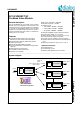
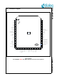
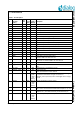
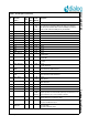
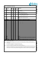
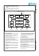
Table Of Contents
- 1.0 Connection diagram
- 2.0 Introduction
- 3.0 Cordless Voice Module functionality
- 4.0 Functional description
- 5.0 CAT-iq
- 6.0 Specifications
- 6.1 General
- 6.2 Absolute Maximum ratings
- 6.3 Operating Conditions
- 6.4 Digital Input/Output Pins
- 6.5 Analog Front End
- Table 11: Microphone amplifier
- Table 12: Microphone amplifier (Operating Condition)
- Table 13: Microphone supply voltages
- Table 14: VREFp load circuit
- Table 15: LSRp/LSRn outputs
- Table 16: LSRp/LSRn load circuits
- Table 17: PAOUTp, PAOUTn outputs
- Table 18: PAOUTp, PAOUTn outputs (Note 19)
- Table 19: PAOUTp, PAOUTn external components
- 6.6 Battery management
- 6.7 Baseband Part
- 6.8 Radio (RF) Part
- 6.9 RF Power supply
- 6.10 RF channel frequencies
- 7.0 Design guidelines
- 8.0 Example Application Diagram
- 9.0 Notices to OEM
- 10.0 Package information
- 11.0 Revision history

SC14CVMDECT SF Cordless Voice Module
© 2012 Dialog Semiconductor B.V. 6 July 1, 2014 v1.6
28 GND - - - Ground
29 PON I - I (270k
fixed
pull-
down)
Power on, Switches on the device if Voltage > 1.5 V.
May be directly connected to VBAT, also with Li-Ion batteries.
After startup the software takes over then PON pin to keep the
device on after which the PON pin may be released.
30 ULP_XTAL I - I 32.768 kHz XTAL clock input. Connect to GND if not used. (Note 3)
31 ULP_PORT I - I Ultra Low Power Port Pin. Connect to GND if not used. (Note 3)
32 P2[7] IO 8 I-PU I/O port
33 P1[5] IO 8 O-1 I/O Port
34 P1[4] IO 1/2 I-PD I/O port
35 P1[3] IO 1/2 I-PD I/O Port
36 P1[2] IO 2 I-PD I/O Port
37 P1[1] IO 2 I-PU I/O Port
38 GND - - - Ground
39 P2[6] IO 2 I-PU I/O port
40 P0[7] / SPI_DI IO 8 I-PU I/O Port
SPI Data Input
41 P0[6] / SPI_DO IO 8 I-PU I/O Port
SPI Data Out
42 P0[5] / SPI_CLK IO 8 I-PU I/O Port
SPI Clock
43 P0[4] / SPI_EN IO 8 I-PU I/O port
SPI_EN: Active low.
44 P0[3] / SCL2 /
URX2
IO 8 I-PU I/O port
Access bus clock, UART Serial In.
45 GND - - - Ground
46 P0[2] / SDA2 /
UTX2
IO 8 I-PU I/O port
Access bus data, UART Serial Out.
47 P0[1] / URX IO 8 I-PD
(10k)
I/O port
UART Serial In
48 P0[0] / UTX O 8 I-PU I/O Port
UART Serial Out
49 GND - - - Ground
50 GND - - - Ground
51 GND - - - Ground
52 RSTn I 1 I-PU
(200k
pull-up)
Active low Reset input with Schmitt-trigger input, open-drain output
and pull up resistor to internal VDD. Input may not exceed 2.0 V. An
internal capacitor of 47 nF is mounted on this pin.
53 JTAG IO 8 I-PU JTAG-SDI+; one wire Debug interface with open-drain.
Requires external 1 k pull-up to VDD.
54 P2[5]/PCM_FSC IO 8 I-PU I/O Port
PCM_FSC: PCM Frame Sync
55 P2[4]/SCL1/
PCM_DO
IO 8 I-PU I/O port
SCL1; I2C clock
PCM_DO: PCM Data output
Table 1: Pin description (Continued)
Pin
Module
Pin name
(Note 1)
In/
Out
Iout
Drive
(mA)
Reset
State
(Note 2)
Description