
User's Manual
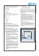
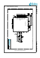
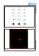
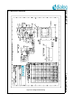
Table Of Contents
- 1.0 Connection diagram
- 2.0 Introduction
- 3.0 Cordless Voice Module functionality
- 4.0 Functional description
- 5.0 CAT-iq
- 6.0 Specifications
- 6.1 General
- 6.2 Absolute Maximum ratings
- 6.3 Operating Conditions
- 6.4 Digital Input/Output Pins
- 6.5 Analog Front End
- Table 11: Microphone amplifier
- Table 12: Microphone amplifier (Operating Condition)
- Table 13: Microphone supply voltages
- Table 14: VREFp load circuit
- Table 15: LSRp/LSRn outputs
- Table 16: LSRp/LSRn load circuits
- Table 17: PAOUTp, PAOUTn outputs
- Table 18: PAOUTp, PAOUTn outputs (Note 19)
- Table 19: PAOUTp, PAOUTn external components
- 6.6 Battery management
- 6.7 Baseband Part
- 6.8 Radio (RF) Part
- 6.9 RF Power supply
- 6.10 RF channel frequencies
- 7.0 Design guidelines
- 8.0 Example Application Diagram
- 9.0 Notices to OEM
- 10.0 Package information
- 11.0 Revision history

SC14CVMDECT SF Cordless Voice Module
© 2012 Dialog Semiconductor B.V. 41 July 1, 2014 v1.6
For a FP hardware design the following hardware parts
will be needed besides the SC14CVMDECT SF:
• Supply voltage
• Battery charge
• LED and buttons
• Audio:
• Headset
• External PCM device.
For a PP hardware design the following hardware parts
will be needed besides the SC14CVMDECT SF:
• Power
• Battery Charger
• Audio:
• Microphone
• Earpiece
• Speaker
• Headset
7.3.2 PCB Design Guidelines
• Because of the presence of the digital radio fre-
quency burst with 100 Hz time division periods (TDD
noise), supply ripple and RF radiation, special atten-
tion is needed for the power supply and ground PCB
layout.
• Power supply considerations
Both high and low frequency bypassing of the supply
line connections should be provided and placed as
close as possible to the SC14CVMDECT SF. In
order to get the best overall performance for both FP
and PP applications, a number of considerations for
the PCB has to be taken into account.
• Make angle breaks on long supply lines to avoid
resonance frequencies in respect to DECT fre-
quencies. Maximum 8 cm before an angle break
is recommended.
• Supply lines should be placed as far as possible
away from sensitive audio circuits. If it is neces-
sary to cross supply lines and audio lines, it
should be done with right angles between supply
and audio lines/circuits (microphone, ear-speaker,
speakerphone, etc.)
• Ground plane considerations
In order to achieve the best audio performance
and to avoid the influence of power supply noise,
RF radiation, TDD noise and other noise sources,
it is important that the audio circuits on both FP
and PP applications boards are connected to the
VREFM pin (analog ground: AGND, see Figure
38) on the SC14CVMDECT SF with separate nets
in the layout.
It is advised to provide the following audio circuits
with separate ground nets connected to the
VREFM pin:
• Microphone(s)
• Headset microphone and speaker
• Speakerphone (signal grounds)
Depending on the layout it may also be necessary to
bypass a number of the audio signals listed above to
avoid humming, noise from RF radiation and TDD
noise with. It is also important to choose a microphone
of appropriate quality with a high RF immunity (with
built-in capacitor).
• ESD performance
Besides TDD noise, the ESD performance is impor-
tant for the end-application. In order to achieve a
high ESD performance supply lines should be
placed with a large distance from charging terminals,
display, headset connector and other electrical ter-
minals with direct contact to the ESD source.
On a two-layer PCB application it is important to
keep a simulated one layer ground. With a stable
ground ESD and TDD noise performance will always
improve.
• Clearance around test patterns
Pin number 81 to 88 are used for production test
purposes. In order to avoid any interference or dis-
turbance the area around these signal pins must be
kept clear of any signal and/or GND. The recom-
mended clearance is at least 1 mm as shown in Fig-
ure 36.
Figure 36 Clearance around test patterns
Test
pattern
0.9mm
0.6mm1.0mm
1.0mm
GND Pattern