
User's Manual
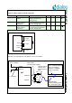
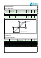
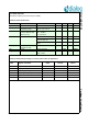
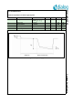
Table Of Contents
- 1.0 Connection diagram
- 2.0 Introduction
- 3.0 Cordless Voice Module functionality
- 4.0 Functional description
- 5.0 CAT-iq
- 6.0 Specifications
- 6.1 General
- 6.2 Absolute Maximum ratings
- 6.3 Operating Conditions
- 6.4 Digital Input/Output Pins
- 6.5 Analog Front End
- Table 11: Microphone amplifier
- Table 12: Microphone amplifier (Operating Condition)
- Table 13: Microphone supply voltages
- Table 14: VREFp load circuit
- Table 15: LSRp/LSRn outputs
- Table 16: LSRp/LSRn load circuits
- Table 17: PAOUTp, PAOUTn outputs
- Table 18: PAOUTp, PAOUTn outputs (Note 19)
- Table 19: PAOUTp, PAOUTn external components
- 6.6 Battery management
- 6.7 Baseband Part
- 6.8 Radio (RF) Part
- 6.9 RF Power supply
- 6.10 RF channel frequencies
- 7.0 Design guidelines
- 8.0 Example Application Diagram
- 9.0 Notices to OEM
- 10.0 Package information
- 11.0 Revision history

SC14CVMDECT SF Cordless Voice Module
© 2012 Dialog Semiconductor B.V. 33 July 1, 2014 v1.6
Note 18: 0 dBm0 on CIN = -3.14 dB of max PCM value.
Table 14: VREFp load circuit
PARAMETER DESCRIPTION CONDITIONS MIN TYP MAX UNIT
Cload_vrefp VREFp (parasitic) load
capacitance
20 pF
Iout_vrefp VREFp output current 1 mA
Figure 29 VREFp load circuit
C
load_vrefp
VREFp
VREFm
Iout_vrefp
Rout_vrefp
Table 15: LSRp/LSRn outputs
PARAMETER DESCRIPTION CONDITIONS MIN TYP MAX UNIT
Vlsr_0dB_unt Untrimmed differen-
tial RMS output volt-
age between LSRp
and LSRn in audio
mode (0 dBm0 refer-
ence level)
0 dBm0 on CIN (Note 18),
LSRATT[2:0] = 001,
@ 1020 Hz Load circuit A (see
Figure 30, Table 16) with
RL1= , Cp1 or load circuit
B (see Figure 31) with RL2,
Cp2 and Cs2
Tolerance:
• 13% when untrimmed
(
BANDGAP_REG=8)
• 6% when trimmed
(Note 16)
621 714 807 mV
Rout_lsr Resistance of acti-
vated loudspeaker
amplifier outputs
LSRp and LSRn
1
Vlsr_dc DC offset between
LSRp and LSRn
(Note 7)
LSRATT[2:0] = 3
R
L1
= 28
3 sigma deviation limits
-20 20 mV