
User's Manual
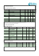
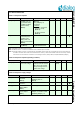
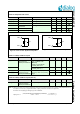
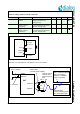
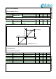
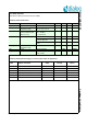
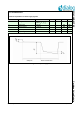
Table Of Contents
- 1.0 Connection diagram
- 2.0 Introduction
- 3.0 Cordless Voice Module functionality
- 4.0 Functional description
- 5.0 CAT-iq
- 6.0 Specifications
- 6.1 General
- 6.2 Absolute Maximum ratings
- 6.3 Operating Conditions
- 6.4 Digital Input/Output Pins
- 6.5 Analog Front End
- Table 11: Microphone amplifier
- Table 12: Microphone amplifier (Operating Condition)
- Table 13: Microphone supply voltages
- Table 14: VREFp load circuit
- Table 15: LSRp/LSRn outputs
- Table 16: LSRp/LSRn load circuits
- Table 17: PAOUTp, PAOUTn outputs
- Table 18: PAOUTp, PAOUTn outputs (Note 19)
- Table 19: PAOUTp, PAOUTn external components
- 6.6 Battery management
- 6.7 Baseband Part
- 6.8 Radio (RF) Part
- 6.9 RF Power supply
- 6.10 RF channel frequencies
- 7.0 Design guidelines
- 8.0 Example Application Diagram
- 9.0 Notices to OEM
- 10.0 Package information
- 11.0 Revision history

SC14CVMDECT SF Cordless Voice Module
© 2012 Dialog Semiconductor B.V. 32 July 1, 2014 v1.6
6.5 ANALOG FRONT END
Note 14: BANDGAP_REG will be tuned at the factory.
Note 15: 0 dBm0 on COUT = -3.14 dB of max PCM value. COUT is CODEC output in test mode
Note 16: Trimming possibility is foreseen. At system production the bandgap reference voltage can be controlled within 2% accuracy and data can
be stored in Flash. Either AVD or VREF can be trimmed within 2% accuracy. If AVD is trimmed VREF will be within 2% accuracy related to
either AVD. Or vice versa VREF can be trimmed. For Vref trimming measure
VREFp, VREFm) and update BANDGAP_REG[3..0].
Note 17: Vrefm is a clean ground input and is the 0 V reference.
Table 11: Microphone amplifier
PARAMETER DESCRIPTION CONDITIONS MIN TYP MAX UNIT
Vmic_0dB_unt Untrimmed differen-
tial RMS input volt-
age between MICp
and MICn (0 dBm0
reference level)
(Note 7)
0 dBm0 on COUT
(Note 15)
MIC_GAIN[3:0] = 0,
@ 1020 Hz;
Tolerance:
• 13% when untrimmed
(
BANDGAP_REG=8)
(Note 14)
• 6% when trimmed
(Note 16)
114 131 149 mV
Rin_mic Resistance of acti-
vated microphone
amplifier inputs
(MICp, MICn and
MICh) to internal GND
(Note 7)
75 150 k
Vmic_offset Input referred DC-off-
set (Note 7)
MIC_GAIN[3..0] = 1111
3 sigma deviation limits
-2.6 +2.6 mV
Table 12: Microphone amplifier (Operating Condition)
PARAMETER DESCRIPTION CONDITIONS MIN TYP MAX UNIT
Vmic_cm_level MICp and MICn com-
mon mode voltage
MICp and MICn are set to
GND with internal resistors
(Rin_mic). If DC coupled
the input voltage must be
equal to this voltage.
(0.9 V/1.5)*
VREFp
V
Table 13: Microphone supply voltages
PARAMETER DESCRIPTION CONDITIONS MIN TYP MAX UNIT
Vref_unt VREFp-VREFm
untrimmed
(Note 17)
I
LOAD
= 0 mA
BANDGAP_REG = 8
(Note 16)
1.41 1.5 1.59 V
Rout_vrefp VREFp output
resistance
Figure 29 1
Nvrefp_idle Peak noise on
VREFp-VREFm
(Note 7)
CCITT weighted -120 dBV
PSRRvrefp Power supply rejec-
tion Vref output
(Note 7)
See Figure 29, AVD to
VREFp/m, f = 100 Hz to 4 kHz
BANDGAP_REG[5:4] = 3
40 dB