
User's Manual
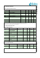
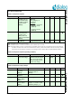
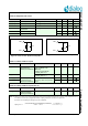
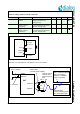
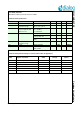
Table Of Contents
- 1.0 Connection diagram
- 2.0 Introduction
- 3.0 Cordless Voice Module functionality
- 4.0 Functional description
- 5.0 CAT-iq
- 6.0 Specifications
- 6.1 General
- 6.2 Absolute Maximum ratings
- 6.3 Operating Conditions
- 6.4 Digital Input/Output Pins
- 6.5 Analog Front End
- Table 11: Microphone amplifier
- Table 12: Microphone amplifier (Operating Condition)
- Table 13: Microphone supply voltages
- Table 14: VREFp load circuit
- Table 15: LSRp/LSRn outputs
- Table 16: LSRp/LSRn load circuits
- Table 17: PAOUTp, PAOUTn outputs
- Table 18: PAOUTp, PAOUTn outputs (Note 19)
- Table 19: PAOUTp, PAOUTn external components
- 6.6 Battery management
- 6.7 Baseband Part
- 6.8 Radio (RF) Part
- 6.9 RF Power supply
- 6.10 RF channel frequencies
- 7.0 Design guidelines
- 8.0 Example Application Diagram
- 9.0 Notices to OEM
- 10.0 Package information
- 11.0 Revision history

SC14CVMDECT SF Cordless Voice Module
© 2012 Dialog Semiconductor B.V. 31 July 1, 2014 v1.6
6.3 OPERATING CONDITIONS
Note 10: Within the specified limits, a life time of 10 years is guaranteed.
Note 11: A life time of 10 years of the CLASS-D amplifier is guaranteed if switched on for 10% of the time.
Note 12: Within this temperature range full operation is guaranteed.
6.4 DIGITAL INPUT/OUTPUT PINS
Note 13: For output drive capability, see section "Pin Description" on page 5.
Table 8: Operating Conditions (Note 10)
PARAMETER DESCRIPTION CONDITIONS MIN TYP MAX UNIT
Vbat Supply voltage on pin VBATIN 2.1 3.45 V
Vdd_pa CLASSD supply voltage on pin VDDPA 2.1 3.45 V
Vpon Voltage on pin PON 5.5 V
Vdig_bp Voltage on digital pins with back drive
protection; ports P0 and P2 (except P2.6)
3.45 V
Vdig Voltage on other digital pins VDD = 1.8 V 1.98 V
Vana Voltage on analog pins AVD = 1.8 V 2.1 V
Icharge Current through pin CHARGE Rseries >
(Vcharge-3 V)/
10 mA
10 mA
Ipa Current through pin PAOUTp, PAOUTn (Note 11) 500 mA
Iout_vrefp Output current through pin VREFp 1 mA
TA Ambient temperature (Note 12) -40 +85 °C
Table 9: Digital input levels
PARAMETER DESCRIPTION CONDITIONS MIN TYP MAX UNIT
Vil_dig Logic 0 input level; all digital
input pins except PON,
CHARGE and RSTn
VDD = 1.8 V 0.3*VDD V
Vil_pon Logic 0 input level; pin PON 0.9 V
Vil_charge Logic 0 input level; pin
CHARGE
0.9 V
Vil_rst Logic 0 input level; pin RSTn VDD = 1.8 V 0.2*VDD V
Vih_dig Logic 1 input level; all digital
input pins except PON,
CHARGE and RSTn
VDD = 1.8 V 0.7*VDD V
Vih_pon Logic 1 input level; pin PON 1.5 V
Vih_charge Logic 1 input level; pin
CHARGE
1.5 V
Vih_rst Logic 1 input level; pin RSTn VDD = 1.8 V 0.8*VDD V
Table 10: Digital output levels
PARAMETER DESCRIPTION CONDITIONS MIN TYP MAX UNIT
Vol_dig Logic 0 output level VDD = 1.8 V; Iout =
2, 4, 8 mA (Note 13)
0.2*VDD V
Voh_dig Logic 1 output level VDD = 1.8 V; Iout =
2, 4, 8 mA (Note 13)
0.8*VDD V