
User's Manual
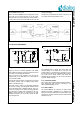
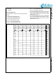
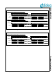
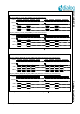
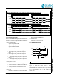
Table Of Contents
- 1.0 Connection diagram
- 2.0 Introduction
- 3.0 Cordless Voice Module functionality
- 4.0 Functional description
- 5.0 CAT-iq
- 6.0 Specifications
- 6.1 General
- 6.2 Absolute Maximum ratings
- 6.3 Operating Conditions
- 6.4 Digital Input/Output Pins
- 6.5 Analog Front End
- Table 11: Microphone amplifier
- Table 12: Microphone amplifier (Operating Condition)
- Table 13: Microphone supply voltages
- Table 14: VREFp load circuit
- Table 15: LSRp/LSRn outputs
- Table 16: LSRp/LSRn load circuits
- Table 17: PAOUTp, PAOUTn outputs
- Table 18: PAOUTp, PAOUTn outputs (Note 19)
- Table 19: PAOUTp, PAOUTn external components
- 6.6 Battery management
- 6.7 Baseband Part
- 6.8 Radio (RF) Part
- 6.9 RF Power supply
- 6.10 RF channel frequencies
- 7.0 Design guidelines
- 8.0 Example Application Diagram
- 9.0 Notices to OEM
- 10.0 Package information
- 11.0 Revision history

SC14CVMDECT SF Cordless Voice Module
© 2012 Dialog Semiconductor B.V. 27 July 1, 2014 v1.6
4.12.7 PCM Interface for PP
The SC14CVMDECT SF supports PCM interface func-
tionality to connect to an external audio source/destina-
tion. Refer to document [2] for detailed information.
• PCM interface mode
supports only master mode.
• PCM_FSC frequency
supports 8 kHz and 16 kHz.
• LENGTH of PCM_FSC
The PCM interface supports the following options:
• 1: The length of PCM_FSC pulse is equal to 1
data bit.
• 8: The length of PCM_FSC pulse is equal to 8
data bits.
• 16: The length of PCM_FSC pulse is equal to 16
data bits.
• 32: The length of PCM_FSC pulse is equal to 32
data bits.
• Start position of FSC
The PCM interface supports the following options:
• The FSC pulse starts 1 data bit before MSB bit of
the PCM channel 0 data.
• The FSC pulse starts at the same time as the
MSB bit of the PCM channel 0 data.
• PCM clock
PCM clock is delivered to an external slave PCM
device from SC14CVMDECT SF.
• PCM Data mode
Supports only linear 16 bit PCM.
4.13 ANTENNA OPERATION
Figure 27 shows the internal circuit of the
SC14CVMDECT SF. Pin RF0 is used for two external
antennas and can also be used for RF test purposes,
so it is recommended to add a 10 pF capacitor as
reserve pattern even when the two external antennas
are not used.
Figure 26 PCM bus with compressed wideband using A-law/ -law, G726 used on air interface
PCM CLK
16 KHz FSC
PCM in
PCM out
Channel 0
Channel 0
Channel 1
Channel 1
Channel 0
Channel 0
Channel 1
Channel 1
AP_DATA_FORMAT_CWB_ALAW / AP_DATA_FORMAT_CWB_ULAW with 16 kHz frame sync (G.726 on air):
1
st
frame
1
st
frame
1
st
frame
1
st
frame
PCM CLK
8 KHz FSC
PCM in
PCM out
Channel 0
Channel 0
Channel 1
Channel 1
Channel 0
Channel 0
Channel 1
Channel 1
Channel 0
Channel 0
Channel 1
Channel 1
Channel 0
Channel 0
Channel 1
Channel 1
AP_DATA_FORMAT_CWB_ALAW / AP_DATA_FORMAT_CWB_ULAW with 8 kHz frame sync (G.726 on air):
1
st
frame
1
st
frame
2
nd
frame
2
nd
frame
1
st
frame
1
st
frame
2
nd
frame
2
nd
frame
2
nd
frame
2
nd
frame
2
nd
frame
2
nd
frame
1
st
frame
1
st
frame
1
st
frame
1
st
frame
1
st
frame
1
st
frame
1
st
frame
1
st
frame
Figure 27 Internal circuit of the SC14CVMDECT SF
RF1
TP1
Internal antenna
RF0
P0n
P0
TX
RX
RFP0n
RFP0