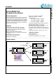
DATASHEET SC14CVMDECT SF Cordless Voice Module General description n n The SC14CVMDECT SF is a member of the Cordless Module family with integrated radio transceiver and baseband processor in a single package. It is designed for hosted and embedded cordless voice and data applications in the DECT frequency band. Its simple to use API commands allow easy setup of a wireless link between two or more nodes.
1.0 Connection diagram. . . . . . . . . . . . . . . . . . . . . . . . 4 4.9 BATTERY MANAGEMENT . . . . . . . . . . . . . . . 21 1.1 PIN DESCRIPTION . . . . . . . . . . . . . . . . . . . . . . 5 4.10 PROTOCOL STACK . . . . . . . . . . . . . . . . . . 21 4.10.1 DECT TBR22 . . . . . . . . . . . . . . . . . . . . 21 2.0 Introduction . . . . . . . . . . . . . . . . . . . . . . . . . . . . . . 8 4.10.2 Out-of-Range handling. . . . . . . . . . . . . 22 2.1 SCOPE . . . . . . . . . . . . . . . . . . . . . . .
SC14CVMDECT SF Table of Contents 42 7.5 PATTERN FOR PIN 79 ON THE MAIN BOARD. 42 7.6 PRECAUTIONS REGARDING UNINTENDED COUPLING . . . . . . . . . . . . . . . . . . . . . . . . . . . 42 8.0 Example Application Diagram. . . . . . . . . . . . . . . 43 9.0 Notices to OEM. . . . . . . . . . . . . . . . . . . . . . . . . . . 44 9.1 FCC REQUIREMENTS REGARDING THE END PRODUCT AND THE END USER. . . . . . . . . . 44 9.2 IC REQUIREMENTS REGARDING THE END PRODUCT AND THE END USER . . . . . . . . . 44 9.
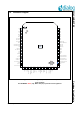
SC14CVMDECT SF Connection diagram 79 TP1 GND 1 78 GND P0 2 77 GND RFP0 3 76 GND P0n 4 75 RF0 RFP0n 5 74 GND GND 6 73 RF1 VREFp 7 72 GND MICp/CIDINn 8 71 GND MICn/CIDOUT 9 70 GND MICh/LINEIN 10 69 PARADET/P3[4] VREFm 11 68 RINGOUT/RINGING/P3[5] LSRp/LINEOUT/AGND 12 67 RINGn/P3[6] LSRn/LINEOUT/AGND 13 66 RINGp/P3[7] GND 14 65 CIDINp/P3[2] ADC0/P3[3] 15 64 VBATIN ADC1/INT0/P1[0] 16 63 VBATIN SOCp 17 62 VBATSW SOCn 18 61 VDDOUT DC_SENSE
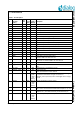
SC14CVMDECT SF 1.1 PIN DESCRIPTION Table 1: Pin description Pin Module Pin name (Note 1) 1 GND - - - 2 P0 O 8 Hi-Z 3 RFP0 O 8 Hi-Z Control port for FAD. See 4.13 4 P0n O 8 Hi-Z Control port for FAD. See 4.13 5 RFP0n O 8 Hi-Z Control port for FAD. See 4.13 In/ Out Iout Reset Drive State Description (mA) (Note 2) Ground Control port for FAD. See 4.
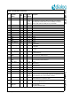
Pin Module Pin name (Note 1) 28 GND - - - 29 PON I - I (270k fixed pulldown) 30 ULP_XTAL I - I 32.768 kHz XTAL clock input. Connect to GND if not used. (Note 3) 31 ULP_PORT I - I Ultra Low Power Port Pin. Connect to GND if not used. (Note 3) 32 P2[7] IO 8 I-PU I/O port 33 P1[5] IO 8 O-1 I/O Port In/ Out Iout Reset Drive State Description (mA) (Note 2) Ground Power on, Switches on the device if Voltage > 1.5 V.
SC14CVMDECT SF Table 1: Pin description (Continued) Pin Module Pin name (Note 1) In/ Out Iout Reset Drive State Description (mA) (Note 2) 56 P2[3]/SDA1 / PCM_DI IO 8 I-PU I/O Port SDA1: I2C Data PCM_DI: PCM Data input 57 P2[2]/PCM_CLK I/O 8 I-PD I/O Port PCM_CLK: PCM clock input/output 58 P2[1] / PWM1 / LED4 IO 8 I I/O Port PWM1: Pulse Width Modulation output LED4: 2.5 mA/5 mA LED current sink 59 P2[0]/ PWM0 / LED3 IO 8 I I/O Port PWM0: LED3: 2.
Introduction 2.1 SCOPE The SC14CVMDECT SF is a programmable DECT module for voice and data services. The internal software stack receives commands and data from the application, for instance to set up a link to other modules. The application software can be implemented on the module itself or on an external host processor. The internal FLASH provides user space where custom applications can be located.
SC14CVMDECT SF VES Virtual EEPROM Storage Walkie Talkie Call between two PPs without an FP Cordless Voice Module © 2012 Dialog Semiconductor B.V. 9 July 1, 2014 v1.
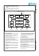
SC14CVMDECT SF 3.0 Cordless Voice Module functionality This section describes the key functions and features supported by the SC14CVMDECT SF as shown in Figure 2. UART interface to host API commands FLASH User SW UART XTAL Phoenix Host API SPI Protocol Stack DSP Radio CODEC / PCM DECT RF Head Set PCM Port Ports Port Pins Figure 2 SC14CVMDECT SF functional overview 3.
Ports SC14CVMDECT SF 3.4 PORTABLE PART CONFIGURATION A Portable Part configuration with SC14CVMDECT SF requires additional external parts as shown in Figure 3. . PCM Loudspeaker UART MCU SC14CVMDECT Earpiece (handset) MIC (handset) Headset Figure 3 PP configuration Table 2 provides an overview of the supported interfaces for a portable part.
SC14CVMDECT SF . Ports PCM Loudspeaker UART MCU SC14CVMDECT Earpiece (handset) MIC (handset) Headset Supply Regulator Figure 4 FP configuration Table 3 provides the overview of required and available interfaces for a basic or a feature rich cordless FP with the SC14CVMDECT SF. . Table 3: FP support overview Item Supported Remark Supply Regulator No Use external 3.
SC14CVMDECT SF G.726 + 1.6 kbit/s SC14CVMDECT PP SC14CVMDECT FP G.722 + 1.6 kbit/s SC14CVMDECT PP Figure 5 Voice and LDR data communication 54 kbit/s SC14CVMDECT PP SC14CVMDECT FP 54 kbit/s SC14CVMDECT PP © 2012 Dialog Semiconductor B.V. 13 Cordless Voice Module Figure 6 LU10 data application July 1, 2014 v1.
SC14CVMDECT SF 3.9 GENERAL FEATURES Standard FP audio control feature. Table 4: Supported general features PP support FP support Remark Conferencing - Yes Call between FP and 4x PP Intercom Yes Yes Call between FP and 4x PP Walkie Talkie mode Yes - Call between PP and PP without FP Baby monitor Yes - Voice Activated PP. See document reference [2] Voice over PCM interface Yes Yes -law (64 kbit/s), A-law (64 kbit/s), G.726 ADPCM (32 kbit/s), G.
Functional description The UART hardware interface uses only TX/RX (see Figure 7). 4.1 UART INTERFACE The UART is normally used for API commands, but can also be used for software upgrades and debugging. The UART is a full duplex UART with frame type: 1 start bit, 8 data bits (LSB first), 1 stop bit, no parity, up to 115.2 kBd. SC14CVMDECT SF 4.0 TX (serial out), module pin 48 RX (serial in), module pin 47 SC14CVMDECT MCU GND Figure 7 UART hardware configuration Caution: All signals are 1.
plane. From this VREFm star point, one connection is made to the common ground plane. The SC14CVMDECT SF PP audio connections are shown in Figure 8. Refer to "Example Application Diagram" on page 43 for detailed component values. Loudspeaker connection For the handsfree operation a 4 loudspeaker must be connected to the PAOUTp and PAOUTn pins as shown in Figure 9. The VDDPA is the supply pin. . VREFp SC14CVMDECT SF 4.3.
PCMx In Codec In IoCtrl IoCtrl IoCtrl IoCtrl Mask && Mask Mask Shift Mask&& Shift Shift Shift CWB CWB CWB Unpack CWB Unpack Unpack Unpack G711 G711 G711 Decoder G711 Decoder Decoder Decoder PCMx Out Codec Out CWB CWB CWB Pack CWB Unpack Unpack Unpack Mac Rx G726 G726 G726 G726 Decoder Encoder Encoder Encoder Mac Tx G722 G726 G726 G726 Encoder Encoder Encoder Encoder Mac Rx G722 G726 G726 G726 Decoder Encoder Encoder Encoder Mac Tx Mac Unit IoCtrl IoCtrl IoCtrl IoCtrl Mask && Mask Mask Shift Ma
VolSideToneUnit SumUnit VolSideTone Mix_Ain_Tone digitaloutgain PFILT 1-3 or IIRSOS 1-3 Limiter VOLCTRL summ2 TonegenAu_0 Earpiece Rx Filters SC14CVMDECT SF Idle Mode summ1 RMSdetector ToneGen EqUnit_0 Earpiece/Headset Mode Earpiece Pass Through EqUnit_0 ECUnit Rx Filters VolSideToneUnit Echo Canceller PFILT 1-3 or IIRSOS 1-3 B1_OUT SumUnit VolSideTone Mix_Ain_Tone Digital Gain & Limiter A1_IN summ2 summ1 ToneGen Analog AGC Tx Filters RFI Canceller TonegenAu_0 Plvl EC1
SC14CVMDECT SF Figure 13 Handset volume configuration 4.5 PP AUDIO MODES The PP audio handling consists of four audio states (see Figure 14). In these states the audio subsystem is configured for a certain audio mode: 4. Headset mode Selection between the modes is done via API calls; see document reference [2]. The Alert state is for tone playing and is entered automatically when tones are played using the API calls. The Alert state can originate from idle, earpiece, handsfree or headset mode. 1.
In Earpiece mode (Handset speaker) an artificial sidetone is generated. The level of the sidetone can be adjusted and setup in the VES through parameter fields Audio.Earp.Vol.Elementx, SideToneGain and Audio.Heads. Elementx.SideToneGain. In Earpiece mode it is possible to adjust the volume in the Earpiece via API calls. In Earpiece mode the PP audio is routed as shown in Figure 11. CVMDECT PP1 CVMDECT FP MIX 4CH PCM 4.5.
change accordingly. When the SC14CVMDECT SF is configured as a PP, the clock has the same accuracy as the FP clock. When the PP synchronises with a FP, the PP crystal is synchronized with the FP crystal and the PP clock will The accuracy is expected to be within 1 minute for up to 6 weeks without being locked to a FP. SC14CVMDECT SF SC14CVMDECT SF crystal. Figure 17 Clock synchronization 4.9 BATTERY MANAGEMENT V supply V B A T IN LD O V B A T IN V supply SOCp SOCn 100 SOCn CHARGE 0.
checksum error is signalled back to the transmitter and the complete packet is retransmitted. The packet will be retransmitted until it is received correctly, or until the link is closed. When the PP goes in-range or out-of-range a signal is sent from the PP to the MMI software indicating whether the PP is in-lock or is out-of-lock with the FP. More transmitted packets will be received in the same order as they were transmitted. The application must handle flow control, if needed. 4.10.
SC14CVMDECT SF Figure 20 Handling product identities 4.11.2 Deregistration The different PCM interface modes and timings are shown in Figure 21 to 26. Refer to document [1] for detailed information. There are two ways of deregistering a PP from an FP: • Remote FP and PP deregistration The correct way to deregister a PP from an FP is to deregister it remotely in the FP.
• 1.536 MHz • Compressed wideband using A-law, 16 kHz sample rate. The 16 bit PCM data is encoded as two 8 bit audio samples if 8 kHz frame sync is used. Used for wideband calls (G.722). 4.12.6 PCM data mode The PCM interface supports the following PCM data formats: • Compressed wideband using -law, 16 kHz sample rate. The 16 bit PCM data is encoded as two 8 bit audio samples if 8 kHz frame sync is used. Used for wideband calls (G.722). • Linear PCM, 8 kHz sample rate. Used for narrowband calls (G.
SC14CVMDECT SF A P _ D A T A _ F O R M A T _ L IN E A R _ 8 k H z w ith 8 k H z fr a m e s y n c : PCM CLK 8 KHz FSC P C M in 1 s t fra m e C hannel 0 PCM out 1 s t fra m e C hannel 0 1 s t fr a m e C hannel 1 1 s t fr a m e C hannel 1 2 n d fra m e C hannel 0 2 n d fra m e C hannel 1 2 n d fra m e C hannel 0 2 n d fra m e C hannel 1 1 s t fra m e C hannel 0 1 s t fra m e C hannel 1 1 s t fra m e C hannel 0 1 s t fra m e C hannel 1 A P _ D A T A _ F O R M A T _ L IN E A R _ 8 k H z w ith 1 6 k
SC14CVMDECT SF AP_DATA_FORMAT_G711A / AP_DATA_FORMAT_G711U with 8 kHz frame sync: PCM CLK 8 KHz FSC 2nd frame PCM in 1st frame Channel 0 1st frame Channel 1 Channel 0 PCM out 1st frame Channel 0 1st frame Channel 1 Channel 0 2nd frame 2nd frame Channel 1 2nd frame Channel 1 AP_DATA_FORMAT_G711A / AP_DATA_FORMAT_G711U with 16 kHz frame sync: PCM CLK 16 KHz FSC PCM in 1st frame Channel 0 1st frame Channel 1 1st frame Channel 0 1st frame Channel 1 PCM out 1st frame Channel 0 1st frame Channe
SC14CVMDECT SF AP_DATA_FORMAT_CWB_ALAW / AP_DATA_FORMAT_CWB_ULAW with 8 kHz frame sync (G.
SC14CVMDECT SF Re-certification of the SC14CVMDECT SF is required if at least one external antenna is added. On request, Dialog Semiconductor can provide a pre-certified PCB layout for an external antenna circuit. RF1 is also recommended to use and can be connected to the RF cable to be able to do the JPN DECT type approval test. 4.13.1 Internal antenna only The FAD function is not enabled if only the internal antenna is used. In this case pins RFP0, RFP0n, P0 and P0n must be left unconnected. 4.13.
CAT-iq • DTMF and tones • Headset support 5.1 INTRODUCTION • Easy PIN code registration CAT-iq stands for Cordless Advanced Technology, Internet and Quality. It is the new global technology initiative from the DECT Forum, designed for IP-voice services in the next generation networks. CAT-iq is based on the regulatory framework of the mature and reliable DECT technology.
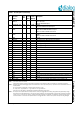
Specifications All MIN/MAX specification limits are guaranteed by design, or production test, or statistical methods unless note 7 is added to the parameter description. Typical values are informative. Note 7: This parameter will not be tested in production. The MIN/MAX values are guaranteed by design and verified by characterization. 6.1 GENERAL Table 6: SC14CVMDECT SF module ITEM CONDITIONS Dimensions lxwxh Weight UNIT 18.0 x 19.6 x 2.7 mm 1.
Table 8: Operating Conditions (Note 10) PARAMETER DESCRIPTION CONDITIONS Vbat Supply voltage on pin VBATIN Vdd_pa CLASSD supply voltage on pin VDDPA Vpon Vdig_bp Vdig Voltage on other digital pins Vana Voltage on analog pins Icharge Current through pin CHARGE Ipa Current through pin PAOUTp, PAOUTn Iout_vrefp Output current through pin VREFp TA Ambient temperature MIN MAX UNIT 2.1 3.45 V 2.1 3.45 V Voltage on pin PON 5.
Table 11: Microphone amplifier PARAMETER DESCRIPTION CONDITIONS MIN TYP MAX UNIT Vmic_0dB_unt Untrimmed differential RMS input voltage between MICp and MICn (0 dBm0 reference level) (Note 7) 0 dBm0 on COUT (Note 15) MIC_GAIN[3:0] = 0, @ 1020 Hz; Tolerance: • 13% when untrimmed (BANDGAP_REG=8) (Note 14) 114 131 149 mV 75 150 SC14CVMDECT SF 6.
PARAMETER DESCRIPTION Cload_vrefp Iout_vrefp Rout_vrefp MAX UNIT VREFp (parasitic) load capacitance 20 pF VREFp output current 1 mA VREFp CONDITIONS MIN TYP SC14CVMDECT SF Table 14: VREFp load circuit Iout_vrefp Cload_vrefp VREFm Figure 29 VREFp load circuit Table 15: LSRp/LSRn outputs PARAMETER DESCRIPTION CONDITIONS MIN TYP MAX UNIT Vlsr_0dB_unt Untrimmed differential RMS output voltage between LSRp and LSRn in audio mode (0 dBm0 reference level) 0 dBm0 on CIN (Note 18), LSRAT
PARAMETER DESCRIPTION CONDITIONS Cp1_Rl1_inf Load capacitance Cp1_Rl1_1k Load capacitance Rl1 Load resistance Cp2 Parallel load capacitance Cs2 Serial load capacitance Rl2 Load resistance MIN TYP MAX UNIT see Figure 30, RL1 = 30 pF see Figure 30, RL1 1 k 100 pF 30 pF 30 F 28 see Figure 31 600 LSRp SC14CVMDECT SF Table 16: LSRp/LSRn load circuits LSRp RL2 RL1 Cp2 Cp1 Cs2 LSRn LSRn Figure 31 Load circuit B: Piezo loudspeaker Figure 30 Load circuit A: Dynami
PARAMETER DESCRIPTION CONDITIONS C_VDDPA Decoupling capacitor on VDDPA Required when Class-D is used and guaranteed life time. (see Figure 32) MIN TYP 1 MAX UNIT F Cs_PAOUT Snubber capacitor (to reduce ringing at PAOUTp/n) Required when Class-D is used to prevent EMI and guaranteed life time. (see Figure 32) 1 nF Rs_PAOUT Snubber resistor (to reduce ringing at PAOUTp/n) Required when Class-D is used to prevent EMI and guaranteed life time.
Table 20: CHARGE_CTRL pin PARAMETER DESCRIPTION CONDITIONS MIN Voh_charge_ctrl Drive capability of pin CHARGE_CTRL sourcing 500 A 1.6 Vol_charge_ctrl TYP MAX UNIT V sinking 100 A 0.2 V MAX UNIT +100 mV Table 21: State of charge circuit (SoC) (Operating condition) DESCRIPTION CONDITIONS MIN Vsocp_socn Input voltage between SOCp and SOCn With the prescribed 0.
Table 23: Radio specifications PARAMETER DESCRIPTION CONDITIONS MIN TYP MAX UNIT P_Rx Receiver sensitivity BER = 0.001; TA = 25 °C -93 -92 -89 dBm P_Rx_T Receiver sensitivity, full temperature range BER = 0.001; -40 °C TA 85 °C -87 dBm IPL Intermodulation performance level (EN 301 406 section 4.5.7.6) TA = 25 °C; Pw = -80 dBm; f = 2 channels NTP Normal transmitted power DECT: 250 mW 24 26 dBm J-DECT: 10 mW average per frame for each slot 23 24.5 dBm 20.
Table 25: Requirements for linear supply regulator PARAMETER DESCRIPTION CONDITIONS MIN TYP MAX UNIT VBAT IN Voltage at VBAT SW Unloaded VB Loaded VB-V1-V2-V3 2.1 3 3.45 V V1 Settling time I = 50 mA 20 mV V2 Receive period I = 130 mA 100 mV V2 Transmit period I = 550 mA 200 mV V3 Drop during transmit 25 mV SC14CVMDECT SF 6.9 RF POWER SUPPLY B Figure 35 RF power supply Cordless Voice Module © 2012 Dialog Semiconductor B.V. 38 July 1, 2014 v1.
SC14CVMDECT SF 6.10 RF CHANNEL FREQUENCIES Table 26: RF frequencies and channel numbers Frequency (MHz) DECT CH 1881.792 9 1883.520 8 1885.248 7 1886.976 6 1888.704 5 1890.432 4 1892.160 3 1893.888 2 1895.616 1 1897.344 0 J-DECT CH DECT6.0 CH 1 0 1899.072 10 1900.800 11 1902.528 12 1921.536 4 1923.264 3 1924.992 2 1926.720 1 1928.448 0 RF setting values must be followed according to AN-D-204 when DECT country mode was changed.
Design guidelines 2. Earpiece mode 3. Handsfree mode (Speakerphone) This section describes the software and hardware considerations to be taken into account when designing the target application. 4. Headset mode Shifting between modes is done through the API. The SC14CVMDECT SF can be used standalone or next to an MCU that controls the module. In case the module is used standalone the application will be stored in its on-board Flash. In total 324 kB of Flash is available for this purpose.
• Microphone(s) • Headset microphone and speaker • Supply voltage • Speakerphone (signal grounds) • Battery charge Depending on the layout it may also be necessary to bypass a number of the audio signals listed above to avoid humming, noise from RF radiation and TDD noise with. It is also important to choose a microphone of appropriate quality with a high RF immunity (with built-in capacitor). • LED and buttons • Audio: • Headset • External PCM device.
Place the module at the edge of the main-board as shown in Figure 37. If the module has to be placed away from the edge of the main board, then avoid conducting areas in front of the antennas and make a cut-out in the main board underneath the antennas as shown in the figure. Keep a distance of at least 10 mm from the antenna elements to conducting objects and at least 5 mm to non-conducting objects. Keep solid ground on layer 2 out to the edges of the main board as shown in the figure.
D C B A 5 J1 J2 5 2 1 1 2 3 4 5 JTAG UTX URX P0[2] P0[3] P0[4] P0[5] P0[6] P0[7] P1[0 P1[1] P1[2] P1[3] P1[4] P1[5] PON CHARGE P2[0] P2[1] P2[2] P2[3] P2[4] P2[5] P2[6] P2[7] PAOUTn PAOUTp P3[2] P3[3] P3[4] P3[5] P3[6] P3[7] internal 22uF C11 + 10pF C12 R9 1K C3 1uF CP_VOUT1 ULP_PORT ULP_XTAL P3[0]/PAOUTn/DP0 P3[1]/PAOUTp/DP1 P3[2]/CIDINp P3[3]/ADC0 P3[4]/PARADET P3[5]/RINGING/RINGOUT P3[6]RINGn P3[7]/RINGp P2[0]/ECZ1/PWM0/LED3 P2[1]/ECZ2/PWM1/LED4 P2[2]/PCM_CLK/CLK100 P2[3]/SDA1/PCM_D
Notices to OEM • Increase the separation between the equipment and receiver The end product has to be certified again if it has been programmed with other software than Dialog standard software stack for portable part and/or uses one or two external antenna(s). • Connect the equipment into an outlet on a circuit different from that to which the receiver is connected. • Consult the dealer or an experienced radio/TV technician for help. 9.1 FCC REQUIREMENTS REGARDING THE END PRODUCT AND THE END USER.
SC14CVMDECT SF 9.3 PRECAUTIONS REGARDING UNINTENDED COUPLING Integration on the main board precautions shall be taken in order to avoid any kind of coupling from the main board to the RF part of the module. If there is any doubt about this, a radio short test should be performed. 9.4 END APPLICATION APPROVAL The module is intended to be used in an end application. Type approval concerning the end product, except for the module, should off cause be done.
SC14CVMDECT SF 10.0 Package information 10.1 SOLDERING PROFILE The SC14CVMDECT SF should be soldered using a standard reflow soldering profile and lead free solder paste as shown below. Adjustments to the profile may be necessary depending on process requirements. Figure 39 Reflow profile 10.
SC14CVMDECT SF 10.3 COPPER PAD, SOLDER OPENING AND STENCIL For the stencil a thickness of 0.122 mm is recommended. Recommended copper pad, solder mask opening and stencil are shown below. Cordless Voice Module Figure 40 Pad dimensions © 2012 Dialog Semiconductor B.V. 47 July 1, 2014 v1.
SC14CVMDECT SF Figure 41 Copper pad, Solder mask opening and Stencil Cordless Voice Module Figure 42 Solder stencil © 2012 Dialog Semiconductor B.V. 48 July 1, 2014 v1.
SC14CVMDECT SF 10.4 MECHANICAL DIMENSIONS Cordless Voice Module Figure 43 Package outline drawing © 2012 Dialog Semiconductor B.V. 49 July 1, 2014 v1.
SC14CVMDECT SF 11.0 Revision history Jul1, 2014 v1.6: • Changed maximum RF output power for DECT 6.0 Apr16, 2014 v1.5 • Added an explanation for RF1 on 4.13 Feb 11, 2014 v1.4 • Correct 10.3Copper pad, solder openinG and STENCIL47 Jan 31, 2014 v1.3 • Update 10.3Copper pad, solder openinG and STENCIL47 Nov 8, 2013 v1.2: • Added section “9.2 INDUSTRY CANADA REQUIREMENTS REGARDING THE END PRODUCT AND THE END USER” Sept 12, 2013 v1.1: • Ordering code for tray version corrected.
Datasheet Status Product Status Definition Advance Information Formative or in Design This data sheet contains the design specifications for product development. Specifications may change in any manner without notice. Preliminary First Production This data sheet contains preliminary data. Supplementary data will be published at a later date. Dialog Semiconductor reserves the right to make changes at any time without notice in order to improve design and supply the best possible product.