
User's Manual

SC14D Reference Design Antenna Product Sheet
Date: October 23, 2013
Page 3 |
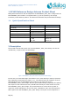
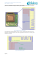
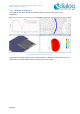
2.1.1 Design Parameters
In order to be allowed to leverage the CVMDECT Modular Approval for the
SC14CVMDECT_AF01_SF01 design, the PCB should meet the following specifications:
• PCB material: FR4
• Dimensions: length x width x thickness = 25.9mm x 25.0mm x 0.8mm
• PCB layer stackup:
• L1 copper thickness: 18um
• L1-L2 prepreg thickness: 163um
• L2 copper thickness: 35um
• L2-L3 core thickness: 360um
• L3 copper thickness: 35um
• L3-L4 prepreg thickness 163um
• L4 copper thickness: 18um
Figure 4. Required layer stackup
The SC14CVMDECT_AF01_SF01 has been designed using 6mil lines/space and 0.25mm
end-size drill holes rules.
When deviating in any way from these specifications, the Modular Approval will be
invalidated and recertification on end-product/system level will be required.