
User's Manual
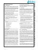
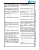
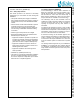
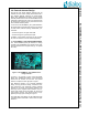
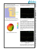

Table Of Contents

AN-D-212 SC14CVMDECT_SFxx_DB External Antenna Design and Leveraging Modular Approval
© 2013 Dialog Semiconductor B.V. Company Confidential 6 June 28, 2013 v0.2
3.1.1 Printed Antenna Design Details
The printed antenna physical design is shown in Figure
2 (noting the 0.5mm grid in the picture).
Figure 2 Printed Antenna Physical Structure
The simulated radiation pattern is depicted in the fol-
lowing plot (with no 0402 component in Figure 2):
Figure 3 Simulated Radiation Pattern
The S11 plot of the SC14CVMDECT_SFxx_DB has
been measured (with no 0402 component in Figure 2)
and is depicted in the following figure:
Figure 4 S11 measurement plot of printed antenna
3.1.2 Tuning Components
For KDECT operation, the frequency band is centered
around 1.8GHz, whereas the default printed antenna
design configuration is designed to be centered
around1.9GHz. The printed antenna design holds a
provision for this shift in operating frequency. Please
refer to Figure 2. If a 100pF capacitor (0402 footprint) is
placed across the gap indicated by the green ellipse
indicated in Figure 2, then effectively the antenna
length is increased resulting in resonant frequency of
1.8GHz (without the 100pF 0402 components, the
antenna’s resonant frequency remains at 1.9GHz for
other DECT operation). No other tuning components
are required.
Figure 5 Printed Antenna Design S11 plot in
KDECT mode
The S11 plot (measured on the actual SC14CVM-
DECT_SFxx_DB Reference Design HW) with the
printed antenna design configured in KDECT mode