
User's Manual
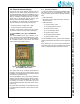
Table Of Contents

AN-D-211 External Antenna Design and Leveraging Modular Approval for CVMDECT
© 2013 Dialog Semiconductor B.V. Company Confidential 6 June 28, 2013 v0.2
3.2 HOST PCB PRINTED ANTENNA DESIGN
The printed antenna that is part of the SC14CVM-
DECT_AF01_SF01 design can also be used directly,
as part of the host PCB design.
In that case, the host PCB design must adhere to the
same PCB layer stackup (material, layer spacings) as
mentioned in section 3.1.1. The antenna must be
located in a corner and spaced from the SC14CVM-
DECT SFxx module in the same way as the
SC14CVMDECT_AF01_SF01 design. Also the ground
plane design (especially the spacing with respect to the
antenna structure) should follow exactly the same out-
line as in the SC14CVMDECT_AF01_SF01 design.
The printed antenna is not 50 Ohms by itself. It
requires a printed transformer on the inner layer (indi-
cated in red in the below picture) that is part of the
SC14CVMDECT_AF01_SF01 design. The layout of
this component is critical to the antenna performance
and should be copied accurately from the available
gerber files.
Figure 2 SC14CVMDECT_AF01_SF01 printed
antenna design details
Figure 2 here above is only meant to show the basic
design; the picture is from simulation used as a basis
for the actual physical design. The gerber files should
be leading in any customer design.
3.3 OTHER ANTENNAS
If an antenna is connected to CVMDECT that has a
dissimilar radation pattern than that of the SC14CVM-
DECT_AF01_SF01 design and/or if the antenna has a
higher gain than that of the SC14CVM-
DECT_AF01_SF01 design, then FCC-04-165 dictates
that the Modular Approval is invalidated and that recer-
tification is required on end-product/system level.
If the antenna connected to CVMDECT is user acces-
sible, then the antenna connector shall be proprietary
(per FCC DA-00-1407).