
User's Manual


UM-B-036
DA14580 Antenna module for QFN48 package
User manual
Revision 2.0
10
-
Dec
-
2014
CFR0012-00 Rev 1 19 of 34 © 2014
Dialog Semiconductor
PCBA
4.16
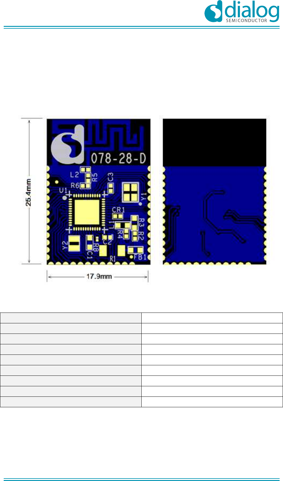
A two-layer FR4 PCB with 1 mm standard thickness is used. The PCB size is 25.4 mm x 17.9 mm.
There are 38 connection pads which are made as castellation (1/2 open drill) with 1.27 mm pitch.
The PCB layout is shown in Figure 15 and the fabrication parameters are given in Table 8.
The schematic diagram and BOM of the QFN48 antenna module are presented in Figure 16 and
Table 9, respectively.
Figure 15: Top view (left) and bottom view (right) of PCBA
Table 8: PCB fabrication parameters
Number of layers
2
Core material
FR4 IMP – 1.0 mm
Top copper thickness
0.018 mm
Bottom copper thickness
0.018 mm
Outer layer track width
0.100 mm
Hole density
<1000 per dm
2
Outer layer isolation distance
0.125 mm
Hole diameter
0.45 mm
Outer layer annular ring
0.100 mm