
User's Manual


UM-B-036
DA14580 Antenna module for QFN48 package
User manual
Revision 2.0
10
-
Dec
-
2014
CFR0012-00 Rev 1 14 of 34 © 2014
Dialog Semiconductor
Table 5: Crystal characteristics
Frequency Accuracy Load capacitance Size Placement
16 MHz ±10 ppm 10 pF 2.5 mm x 2.0 mm Populated
32.768 kHz ±20 ppm 7 pF 3.2 mm x 1.5 mm Optional
Note: When the DC/DC converter configuration is changed to boost mode, a 32.768 kHz crystal
must be mounted. The on-chip RCX oscillator can only be used in buck mode.
OTP programming
4.10
For programming the OTP memory of the DA14580, a DC voltage of 6.7 V (typ.) must be applied to
pin 4 (VPP).
Debugging/testing ports
4.11
Two ports are available for testing/debugging or software development: JTAG and UART: The pin
assignments of these ports are given in Table 6.
Table 6: QFN48 antenna module debug ports
Function
QFN48 antenna module DA14580
Pin name Pin no. Pin name Pin no.
UART transmit (UTX) TxD 13 P0_5 7
UART receive (URX) RxD 12 P0_4 6
JTAG data SWDIO 30 SWDIO 30
JTAG clock SWCLK 31 SWCLK 31
RF section
4.12
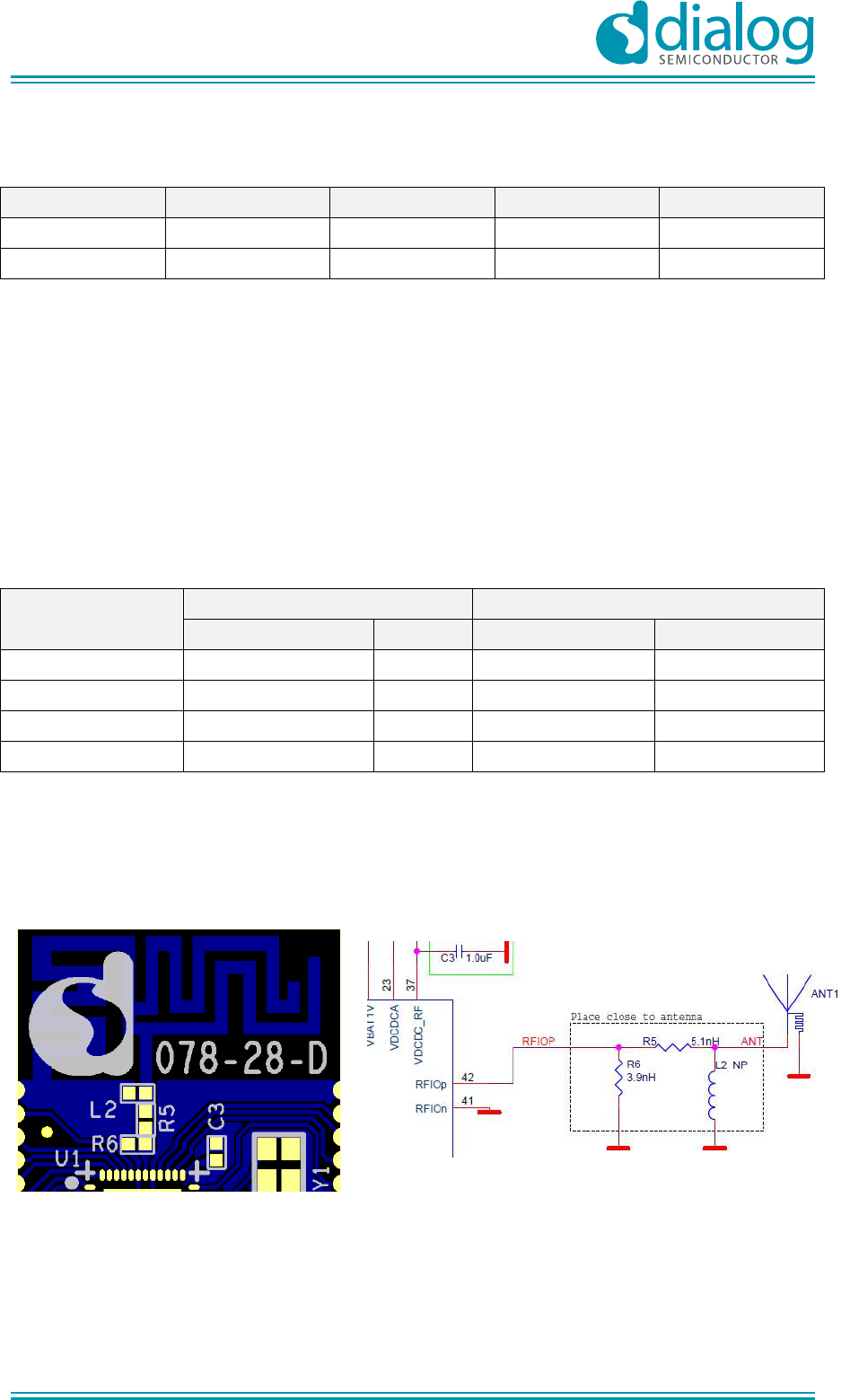
The DA14580 has a single pin RF input/output port. The RF section of the QFN48 antenna module
consists of a printed antenna and the matching network of R5, R6 and L2. L2 is not populated. See
Figure 7.
Figure 7: RF section: PCB layout (left) and schematic (right)
Antenna
4.12.1
A broadband variant of a printed F-antenna is used. A matching network is required for achieving the
maximum power transfer possible. The matching network consists of two inductances: R5 (series
coil: 5.1 nH, 0402, LQP series) and R6 (shunt coil: 3.9 nH, 0402, LQP series).