
User's Manual


UM-B-036
DA14580 Antenna module for QFN48 package
User manual
Revision 2.0
10
-
Dec
-
2014
CFR0012-00 Rev 1 13 of 34 © 2014
Dialog Semiconductor
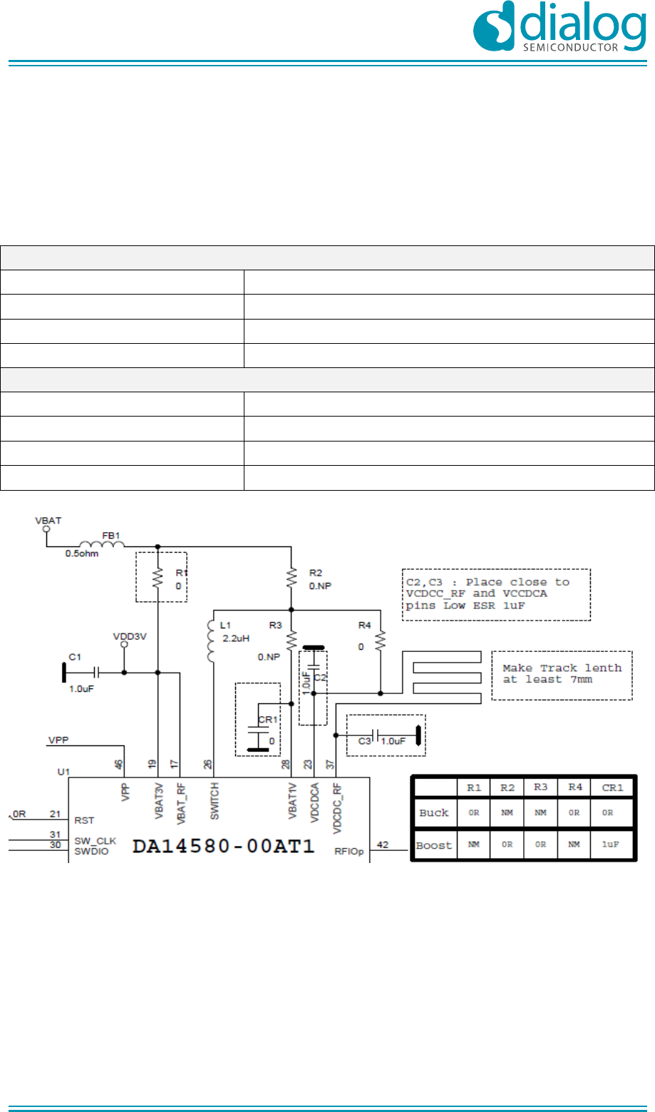
DC/DC converter in boost configuration
4.8.1
Supplying the QFN48 antenna module at a lower voltage (down to 0.9 V) is feasible, but modification
of the module’s components is needed. Please note that this configuration has not been used in the
tests for the FCC/ETSI certification.
Table 4: DA14580 DC/DC converter configurations
Buck configuration (default)
Supply voltage 2.4 V to 3.6 V
Populated components
R1 = 0 Ω, R4 = 0 Ω, CR1 = 0 Ω
Not populated components R2, R3
FCC/CE certification Yes
Boost configuration
Supply voltage 0.9 V to 2.0 V (single cell alkaline battery)
Populated components
R2 = 0 Ω, R3 = 0 Ω, CR1 = 1 µF
Not populated components R1, R4
FCC/CE certification No
Figure 6: DA14580 DC/DC converter circuit
Crystals
4.9
The frequency tolerance specification for BLE is ±50 ppm. To compensate for ageing and offset
effects, the external crystal of 16 MHz must have an accuracy of ±20 ppm or better. On the QFN48
antenna module the 16 MHz crystal (Y1) has a fundamental frequency of 16 MHz ±10 ppm and a
load capacitance of 10 pF. The crystal is located on the module itself. The crystal oscillator frequency
can be tuned using a programmable capacitance bank that is embedded in the DA14580.
For sleep mode the on-chip RCX oscillator is used (typ. 10 kHz). In addition, a 32.768 kHz crystal
(Y2) with a tolerance of ±50 ppm can be mounted on the module.