
User's Manual


UM-B-036
DA14580 Antenna module for QFN48 package
User manual
Revision 2.0
10
-
Dec
-
2014
CFR0012-00 Rev 1 10 of 34 © 2014
Dialog Semiconductor
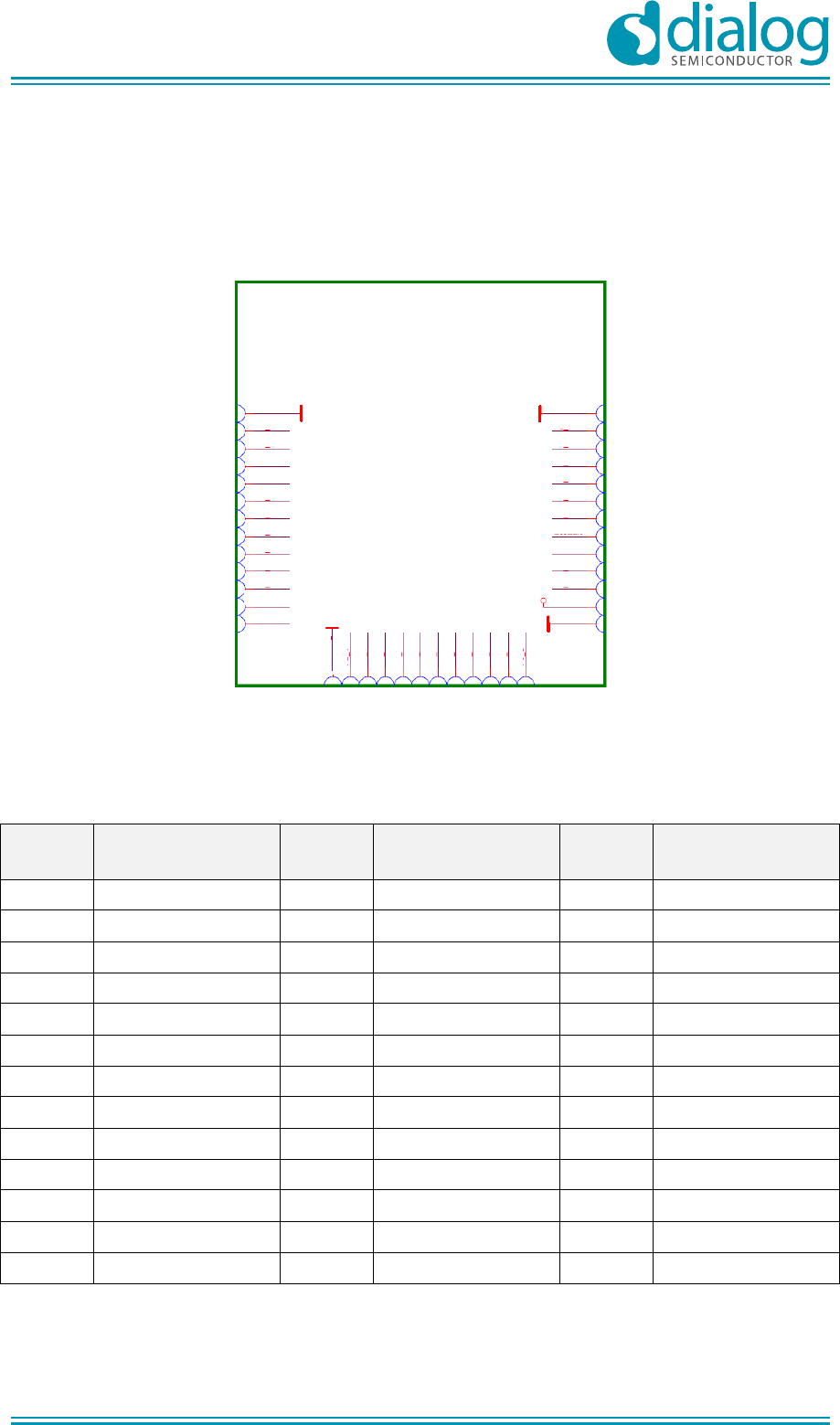
Module pinout
4.6
All available pins of the DA14580 SoC are routed out to the pins of the QFN48 antenna module.
Module pin numbers and names are given in Figure 3 and Table 2. The module pins use the
corresponding names of the DA14580 QFN48 integrated circuit.
1
2
3
4
5
6
7
8
9
10
11
12
13
14
15
16
17
18
19
20
21
22
23
24
25
38
37
36
35
34
33
32
31
30
29
28
27
26
Top View
P2_7
P2_8
VPP
P2_9
P2_0
P0_0
P0_1
P0_2
P0_3
P3_0
TXD/P0_4
RXD/P0_5
GND
P0_6
P3_1
P0_7
P3_2
P3_3
P2_2
P3_4
P2_3
P2_4
P3_5
P2_1
GND
P3_7
P2_6
P2_5
P3_6
P1_3
P1_2
SWCLK
SWDIO
P1_1
P1_0
GND
GND
Vbat
Figure 3: Module pin locations
Table 2: Module pin assignment (top view)
Pin no. Pin name
(PCB left side)
Pin no. Pin name
(PCB bottom side)
Pin no. Pin name
(PCB right side)
1 GND 14 GND 26 GND
2 P2_7 15 P2_1 27 VBAT
3 P2_8 16 P0_6 28 P1_0
4 VPP 17 P3_1 29 P1_1
5 P2_9 18 P0_7 30 SWDIO
6 P2_0 19 P3_2 31 SW_CLK
7 P0_0 20 P3_3 32 P1_2
8 P0_1 21 P2_2 33 P1_3
9 P0_2 22 P3_4 34 P3_6
10 P0_3 23 P2_3 35 P2_5
11 P3_0 24 P2_4 36 P2_6
12 P0_4 (TxD) 25 P3_5 37 P3_7
13 P0_5 (RxD) 38 GND