
Data Sheet
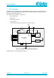
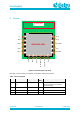
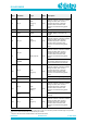
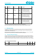
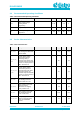
Table Of Contents
- General Description
- Key Features
- Applications
- Contents
- Figures
- Tables
- 1 References
- 2 Block Diagram
- 3 Pinout
- 4 Characteristics
- 5 Mechanical Specifications
- 6 Packaging Information
- 7 Application Information
- 8 Design Guidelines
- 9 Soldering
- 10 Ordering Information
- 11 Regulatory Information
- 12 Environmental Information
- 13 Bluetooth SIG Qualification
- Revision History

DA14531MOD
SmartBond TINY
TM
Module
Preliminary
Datasheet
Revision 2.1
4-June-2020
CFR0011-120-00
9 of 31
© 2020 Dialog Semiconductor
Pin #
Pin Name
Type
Reset
State
Description
J14
P0_5
DIO
(Type B)
I-PD
INPUT/OUTPUT with selectable pull
up/down resistors. Pull-down enabled
during and after reset. General
purpose I/O port bit or alternate
function nodes. Contains state
retention mechanism during power
down.
J15
P0_9
DIO
(Type A)
I-PD
INPUT/OUTPUT with selectable pull
up/down resistors. Pull-down enabled
during and after reset. General
purpose I/O port bit or alternate
function nodes. Contains state
retention mechanism during power
down
J16
P0_8
DIO
(Type A)
I-PD
INPUT/OUTPUT with selectable pull
up/down resistors. Pull-down enabled
during and after reset. General
purpose I/O port bit or alternate
function nodes. Contains state
retention mechanism during power
down.
I-PD stands for Input-Pulled Down while I-PU stands for Input-Pulled Up.
DIO stands for Digital Input-Output, PWR stands for power and GND stands for Ground.
4 Characteristics
All MIN/MAX specification limits are guaranteed by design, production testing and/or statistical
characterization. Typical values are based on characterization results at default measurement
conditions and are informative only.
Default measurement conditions (unless otherwise specified): VBAT= 3.0 V, TA = 25
o
C. All radio
measurements are performed with standard RF measurement equipment.
4.1 Absolute Maximum Ratings
Stresses beyond those listed under Absolute Maximum Ratings may cause permanent damage to
the device. These are stress ratings only, so functional operation of the device at these or any other
conditions beyond those indicated in the operational sections of the specification are not implied.
Exposure to Absolute Maximum Rating conditions for extended periods may affect device reliability.
Table 2: Absolute Maximum Ratings
Parameter
Description
Conditions
Min
Max
Unit
V
BAT_LIM
limiting battery supply voltage
-0.1
3.6
V