
Data Sheet
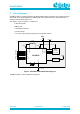
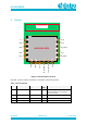
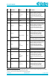
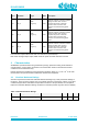
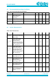
Table Of Contents
- General Description
- Key Features
- Applications
- Contents
- Figures
- Tables
- 1 References
- 2 Block Diagram
- 3 Pinout
- 4 Characteristics
- 5 Mechanical Specifications
- 6 Packaging Information
- 7 Application Information
- 8 Design Guidelines
- 9 Soldering
- 10 Ordering Information
- 11 Regulatory Information
- 12 Environmental Information
- 13 Bluetooth SIG Qualification
- Revision History

DA14531MOD
SmartBond TINY
TM
Module
Preliminary
Datasheet
Revision 2.1
4-June-2020
CFR0011-120-00
8 of 31
© 2020 Dialog Semiconductor
Pin #
Pin Name
Type
Reset
State
Description
J5
P0_6
DIO
(Type A)
Note
1
I-PD
INPUT/OUTPUT with selectable pull
up/down resistors. Pull-down enabled
during and after reset. General
purpose I/O port bit or alternate
function nodes. Contains state
retention mechanism during power
down.
J6
GND
GND
Ground
J7
VBAT
PWR
POWER. Battery connection. IO
supply.
J8
P0_11
DIO
(Type A)
I-PD
INPUT/OUTPUT with selectable pull
up/down resistors. Pull-down enabled
during and after reset. General
purpose I/O port bit or alternate
function nodes. Contains state
retention mechanism during power
down.
J9
P0_10
DIO (Type A)
I-PD
INPUT/OUTPUT with selectable pull
up/down resistors. Pull-down enabled
during and after reset. General
purpose I/O port bit or alternate
function nodes. Contains state
retention mechanism during power
down.
SWDIO
INPUT/OUTPUT. SWI Data
input/output. Bidirectional data and
control communication (by default).
J10
P0_2
DIO
(Type B)
I-PD
INPUT/OUTPUT with selectable pull
up/down resistors. Pull-down enabled
during and after reset. General
purpose I/O port bit or alternate
function nodes. Contains state
retention mechanism during power-
down.
SWCLK
INPUT SWI clock signal (by default).
J11
GND
GND
Ground
J12
P0_0
DIO
(Type B)
Note
2
I-PD
INPUT/OUTPUT with selectable pull
up/down resistors. Pull-down enabled
during and after reset. General
purpose I/O port bit or alternate
function nodes. Contains state
retention mechanism during power-
down
RST
RST active high hardware reset
(default).
J13
P0_7
DIO
(Type A)
I-PD
INPUT/OUTPUT with selectable pull
up/down resistors. Pull-down enabled
during and after reset. General
purpose I/O port bit or alternate
function nodes. Contains state
retention mechanism during power
down.
1
There are two types of pads, namely Type A and Type B. Type A is a normal IO pad with a Schmitt trigger on input while
Type B has an extra RC Filter with a cutoff frequency of 100 kHz.
2
This pin is also used for the communication to the internal SPI FLASH