
Data Sheet
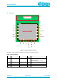
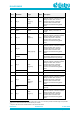
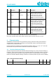
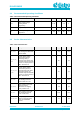
Table Of Contents
- General Description
- Key Features
- Applications
- Contents
- Figures
- Tables
- 1 References
- 2 Block Diagram
- 3 Pinout
- 4 Characteristics
- 5 Mechanical Specifications
- 6 Packaging Information
- 7 Application Information
- 8 Design Guidelines
- 9 Soldering
- 10 Ordering Information
- 11 Regulatory Information
- 12 Environmental Information
- 13 Bluetooth SIG Qualification
- Revision History

DA14531MOD
SmartBond TINY
TM
Module
Preliminary
Datasheet
Revision 2.1
4-June-2020
CFR0011-120-00
7 of 31
© 2020 Dialog Semiconductor
3 Pinout
MARKING AREA
J1
J2
J3
J4
J5
J6 J7 J8 J9 J10 J11
J16
J15
J14
J13
J12
n.c.
GND
GND
GND
P0_6
GND
VBAT
P0_11
P0_10/SWDIO
P0_2/SWCLK
GND
P0_8
P0_9
P0_5/RxTx
P0_7
P0_0/RST
ANTENNA AREA
Figure 2: Pinout Diagram Top View
Note that, J1 has no internal connection, it should be connected to ground.
Table 1: Pin Description
Pin #
Pin Name
Type
Reset
State
Description
J1
n.c
Not internally connected.
Recommended to be connected to
ground externally
J2
GND
GND
Ground
J3
GND
GND
Ground
J4
GND
GND
Ground