
Data Sheet
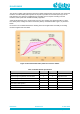
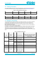
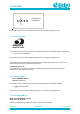
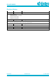
Table Of Contents
- General Description
- Key Features
- Applications
- Contents
- Figures
- Tables
- 1 References
- 2 Block Diagram
- 3 Pinout
- 4 Characteristics
- 5 Mechanical Specifications
- 6 Packaging Information
- 7 Application Information
- 8 Design Guidelines
- 9 Soldering
- 10 Ordering Information
- 11 Regulatory Information
- 12 Environmental Information
- 13 Bluetooth SIG Qualification
- Revision History

DA14531MOD
SmartBond TINY
TM
Module
Preliminary
Datasheet
Revision 2.1
4-June-2020
CFR0011-120-00
22 of 31
© 2020 Dialog Semiconductor
The volume of solder paste applied to the board is mainly determined by the aperture size and stencil
thickness. An initial solder paste aperture for the pads is provided on the solder paste layer of the
PCB footprint. This aperture is modified by the assembly process experts according to stencil
thickness, solder paste and available assembly equipment.
Solder profile depends on the solder paste type used. For example, the soldering profile of a lead-
free solder paste, Sn3Ag0.5Cu with no clean Flux (ROL0) and Solder Powder Type 4, is presented
below.
No clean flux is recommended because washing must not be applied after assembly for avoiding
moisture trapped under the shield.
Figure 21: Recommended reflow profile for Lead Free Solder
Table 11: Reflow profile specification
Statistic name
Low limit
High limit
Units
Slope1 (Target=2.0) Between 30.0 and 70.0
1
3
Degrees/Second
Slope2 (Target=2.0) Between 70.0 and 150.0
1
3
Degrees/Second
Slope3 (Target=-2.8) Between 220.0 and 150.0
-5
-0.5
Degrees/Second
Preheat time 110-190C
60
120
Seconds
Time above reflow @220C
30
65
Seconds
Peak temperature
235
250
Degrees Celsius
Total time above @235C
10
30
Second