
Data Sheet
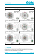
Table Of Contents
- General Description
- Key Features
- Applications
- Contents
- Figures
- Tables
- 1 References
- 2 Block Diagram
- 3 Pinout
- 4 Characteristics
- 5 Mechanical Specifications
- 6 Packaging Information
- 7 Application Information
- 8 Design Guidelines
- 9 Soldering
- 10 Ordering Information
- 11 Regulatory Information
- 12 Environmental Information
- 13 Bluetooth SIG Qualification
- Revision History

DA14531MOD
SmartBond TINY
TM
Module
Preliminary
Datasheet
Revision 2.1
4-June-2020
CFR0011-120-00
21 of 31
© 2020 Dialog Semiconductor
Radiation pattern for antenna trace
Horizontal polarization
Vertical polarization
Figure 15: Radiation pattern for XY-plane, horizontal
polarization.
Figure 16: Radiation pattern for XY-plane, vertical polarization.
Figure 17: Radiation pattern for XZ-plane, horizontal
polarization.
Figure 18: Radiation pattern for XZ-plane, vertical polarization.
Figure 19: Radiation pattern for YZ-plane, horizontal
polarization.
Figure 20: Radiation pattern for YZ-plane, vertical polarization.
9 Soldering
The successful reflow soldering of DA14531 TINY
TM
Module on a PCB depends on several
parameters such as the thickness of the stencil, the pads solder paste aperture, the solder paste
characteristics, the reflow soldering profile, size of the PCB etc.