
Data Sheet
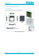
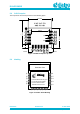
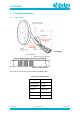
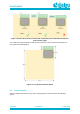
Table Of Contents
- General Description
- Key Features
- Applications
- Contents
- Figures
- Tables
- 1 References
- 2 Block Diagram
- 3 Pinout
- 4 Characteristics
- 5 Mechanical Specifications
- 6 Packaging Information
- 7 Application Information
- 8 Design Guidelines
- 9 Soldering
- 10 Ordering Information
- 11 Regulatory Information
- 12 Environmental Information
- 13 Bluetooth SIG Qualification
- Revision History

DA14531MOD
SmartBond TINY
TM
Module
Preliminary
Datasheet
Revision 2.1
4-June-2020
CFR0011-120-00
14 of 31
© 2020 Dialog Semiconductor
5.2 PCB Footprint
The footprint for the PCB is presented in the following figure:
14.5mm
12.5mm
10.15mm
9.5mm
1.75mm
1.5mm
1mm
2.0mm
2.0mm
0.9mm
Figure 4: Module Footprint Top View
5.3 Marking
Antenna Area
DA14531MOD-00F0100 yyww
FCC ID: Y82-DA14531MOD
IC:9576A-DA14531MOD
ANATEL:0538220-12967
J1
J5
J4
J3
J2
J6
J7
J8
J10
J9
J11
J12
J13
J14
J15
J16
-
Figure 5: Module Shield Marking