
Data Sheet
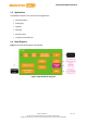

MediaTek MT7681 Datasheet
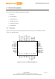
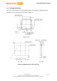
2.2 Pin Descriptions
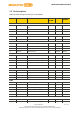
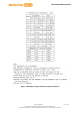
Table 1 provides descriptions of the pins on the MT7681.
QFN40 Pin Name Pin description Default
PU/PD
I/O
Supply
domain
Reset and clocks
24 LDO_RST_N
External system reset for active
low
N/A Input VDD33
37 XTAL_XI Crystal or external clock input N/A Input
36 XTAL_XO Crystal output N/A Input
UART interface
25 UART_RX UART Rx N/A VDD33
26 UART_TX UART Tx N/A VDD33
FLASH interface
8 FLMISO External memory data input PD Input VDD33
9 FLMOSI External memory data output PD Output VDD33
10 FLCS External chip select PU Output VDD33
11 FLCLK External clock PU Output VDD33
Programmable I/O
30 GPIO0 Programmable input/output PD In/out VDD33
31 GPIO1 Programmable input/output PD In/out VDD33
29 GPIO2 Programmable input/output PD In/out VDD33
28 GPIO3 Programmable input/output PD In/out VDD33
27 GPIO4 Programmable input/output PD In/out VDD33
WIFI radio interface
40 BG_EXTR RF BG reference N/A
2 RF_IN RF auxiliary Rx input N/A
4 RF_OUTP RF port N/A
5 RF_OUTN RF port N/A
PMU
17 PMU_12V PMU 1.2V output N/A Output
18 PMU_V15A PMU 1.5V input N/A Input
19, 22 PMU_V33 PMU 3.3V power supply N/A Input
20 PMU_FB PMU control N/A
21 PMU_COMP PMU control N/A
23 PMU_PHASE PMU control N/A
Power supplies
7, 33 VDD33 Digital I/O power supply N/A Input
12, 32 VDD12 Digital core power supply N/A Input
© 2015 MediaTek Inc. Page 7 of 15
This document contains information that is proprietary to MediaTek Inc.
Unauthorized reproduction or disclosure of this information in whole or in part is strictly prohibited.
C