
Data Sheet

MediaTek MT7681 Datasheet
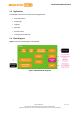
2 Product Descriptions
This section provides details of the MT7681, including:
• Pin layout
• Pin descriptions
• Strapping options
• Package information
• Ordering information
• Top markings
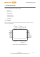
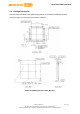
2.1 Pin Layout
Figure 2 shows a top view of the pin layout for the MT7681. These pins are described in detail in
section 2.2, “PIN Description”.
BG_EXTR
RF_LDO
RF_LDO
XTAL_XI
XTAL_XO
RF_LDO
PLL_LDO
VDD33
VDD12
GPIO0
40
39
38
37
36
35
34
33
32
31
RF_LDO
1
30
GPIO1
RF_IN
2
29
GPIO2
RF_V33A
3
28
GPIO3
RF_OUTP
4
27
GPIO4
RF_OUTN
5
26
UART_TX
RF_V33A
6
25
UART_RX
VDD33
7
24
LDO_RST_N
FLMISO
8
23
PMU_PHASE
FLMOSI
9
22
PMU_V33
FLCS
10
21
PMU_COMP
11
12
13
14
15
16
17
18
19
20
FLCLK
VDD12
GND
GND
GND
GND
PMU_12V
PMU_V15A
PMU_V33
PMU_FB
Figure 2 Top view of MT7681 QFN pin-out
© 2015 MediaTek Inc. Page 6 of 15
This document contains information that is proprietary to MediaTek Inc.
Unauthorized reproduction or disclosure of this information in whole or in part is strictly prohibited.
C