
Data Sheet
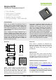


Datasheet SHT20
www.sensirion.com Version 3 – December 2011 4/14
2 Application Information
2.1 Soldering Instructions
The DFN’s die pad (centre pad) and perimeter I/O pads
are fabricated from a planar copper lead-frame by over-
molding leaving the die pad and I/O pads exposed for
mechanical and electrical connection. Both the I/O pads
and die pad should be soldered to the PCB. In order to
prevent oxidation and optimize soldering, the bottom side
of the sensor pads is plated with Ni/Pd/Au.
On the PCB the I/O lands
8
should be 0.2mm longer than
the package I/O pads. Inward corners may be rounded to
match the I/O pad shape. The I/O land width should match
the DFN-package I/O-pads width 1:1 and the land for the
die pad should match 1:1 with the DFN package – see
Figure 8.
The solder mask
9
design for the land pattern preferably is
of type Non-Solder Mask Defined (NSMD) with solder
mask openings larger than metal pads. For NSMD pads,
the solder mask opening should be about 120μm to
150μm larger than the pad size, providing a 60μm to 75μm
design clearance between the copper pad and solder
mask. Rounded portions of package pads should have a
matching rounded solder mask-opening shape to minimize
the risk of solder bridging. For the actual pad dimensions,
each pad on the PCB should have its own solder mask
opening with a web of solder mask between adjacent
pads.
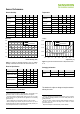
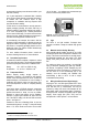
Figure 8 Recommended metal land pattern for SHT2x. Values
in mm. Die pad (centre pad) may be left floating or be connected
to ground, NC pads shall be left floating. The outer dotted line
represents the outer dimension of the DFN package.
For solder paste printing a laser-cut, stainless steel stencil
with electro-polished trapezoidal walls and with 0.125mm
stencil thickness is recommended. For the I/O pads the
stencil apertures should be 0.1mm longer than PCB pads
and positioned with 0.1mm offset away from the centre of
the package. The die pad aperture should cover about 70
– 90% of the pad area – say up to 1.4mm x 2.3mm
8
The land pattern is understood to be the metal layer on the PCB, onto which
the DFN pads are soldered to.
9
The solder mask is understood to be the insulating layer on top of the PCB
covering the connecting lines.
centered on the thermal land area. It can also be split in
two openings.
Due to the low mounted height of the DFN, “no clean”
type 3 solder paste
10
is recommended as well as Nitrogen
purge during reflow.
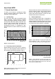
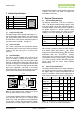
Figure 9 Soldering profile according to JEDEC standard. T
P
<=
260°C and t
P
< 30sec for Pb-free assembly. T
L
< 220°C and t
L
<
150sec. Ramp-up/down speeds shall be < 5°C/sec.
It is important to note that the diced edge or side faces of
the I/O pads may oxidise over time, therefore a solder fillet
may or may not form. Hence there is no guarantee for
solder joint fillet heights of any kind.
For soldering SHT2x, standard reflow soldering ovens may
be used. The sensor is qualified to withstand soldering
profile according to IPC/JEDEC J-STD-020 with peak
temperatures at 260°C during up to 30sec for Pb-free
assembly in IR/Convection reflow ovens (see Figure 9).
For manual soldering contact time must be limited to 5
seconds at up to 350°C.
IMPORTANT: After soldering, the devices should be
stored at >75%RH for at least 12h to allow the sensor
element to re-hydrate. Otherwise the sensor may read an
offset that slowly disappears if exposed to ambient
conditions. Alternatively the re-hydration process may be
performed at ambient conditions (>40%RH) during more
than 5 days.
In no case, neither after manual nor reflow soldering, a
board wash shall be applied. Therefore, and as mentioned
above, it is strongly recommended to use “no-clean” solder
paste. In case of applications with exposure of the sensor
to corrosive gases or condensed water (i.e. environments
with high relative humidity) the soldering pads shall be
sealed (e.g. conformal coating) to prevent loose contacts
or short cuts.
2.2 Storage Conditions and Handling Instructions
Moisture Sensitivity Level (MSL) is 1, according to
IPC/JEDEC J-STD-020. At the same time, it is
10
Solder types are related to the solder particle size in the paste: Type 3 covers
the size range of 25 – 45 µm (powder type 42).
1.0
1.0
0.3
0.4
1.5
0.4
0.7
0.2
0.2
2.4
Temperature
Time
t
P
T
P
T
L
T
S
(max)
t
L
preheating
critical zone