
Data Sheet

Datasheet SHT1x
www.sensirion.com Version 4.3 – May 2010 5/11
resolved by routing VDD and/or GND between the two
data signals and/or using shielded cables. Furthermore,
slowing down SCK frequency will possibly improve signal
integrity. Power supply pins (VDD, GND) must be
decoupled with a 100nF capacitor if wires are used.
Capacitor should be placed as close to the sensor as
possible. Please see the Application Note “ESD, Latch-up
and EMC” for more information.
1.10 ESD (Electrostatic Discharge)
ESD immunity is qualified according to MIL STD 883E,
method 3015 (Human Body Model at 2 kV).
Latch-up immunity is provided at a force current of
100mA with T
amb
= 80°C according to JEDEC78A. See
Application Note “ESD, Latch-up and EMC” for more
information.
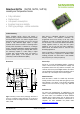
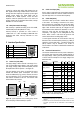
2 Interface Specifications
Pin
Name Comment
1 GND Ground
2 DATA Serial Data, bidirectional
3 SCK Serial Clock, input only
4 VDD Source Voltage
NC
NC Must be left unconnected
Table 1: SHT1x pin assignment, NC remain floating.
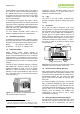
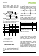
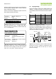
2.1 Power Pins (VDD, GND)
The supply voltage of SHT1x must be in the range of 2.4 –
5.5V, recommended supply voltage is 3.3V. Power supply
pins Supply Voltage (VDD) and Ground (GND) must be
decoupled with a 100 nF capacitor – see Figure 10.
The serial interface of the SHT1x is optimized for sensor
readout and effective power consumption. The sensor
cannot be addressed by I
2
C protocol; however, the sensor
can be connected to an I
2
C bus without interference with
other devices connected to the bus. The controller must
switch between the protocols.
Figure 10: Typical application circuit, including pull up resistor
R
P
and decoupling of VDD and GND by a capacitor.
2.2 Serial clock input (SCK)
SCK is used to synchronize the communication between
microcontroller and SHT1x. Since the interface consists of
fully static logic there is no minimum SCK frequency.
2.3 Serial data (DATA)
The DATA tri-state pin is used to transfer data in and out
of the sensor. For sending a command to the sensor,
DATA is valid on the rising edge of the serial clock (SCK)
and must remain stable while SCK is high. After the falling
edge of SCK the DATA value may be changed. For safe
communication DATA valid shall be extended T
SU
and T
HO
before the rising and after the falling edge of SCK,
respectively – see Figure 11. For reading data from the
sensor, DATA is valid T
V
after SCK has gone low and
remains valid until the next falling edge of SCK.
To avoid signal contention the microcontroller must only
drive DATA low. An external pull-up resistor (e.g. 10kΩ) is
required to pull the signal high – it should be noted that
pull-up resistors may be included in I/O circuits of
microcontrollers. See Table 2 for detailed I/O characteristic
of the sensor.
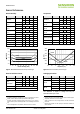
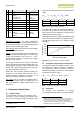
2.4 Electrical Characteristics
The electrical characteristics such as power consumption,
low and high level input and output voltages depend on
the supply voltage. Table 2 gives electrical characteristics
of SHT1x with the assumption of 5V supply voltage if not
stated otherwise.
Parameter Conditions min typ max Units
Power supply DC
10
2.4 3.3 5.5 V
measuring 0.55 1 mA
average
11
2 28 µA
Supply current
sleep 0.3 1.5 µA
Low level output
voltage
I
OL
< 4 mA 0 250 mV
High level output
voltage
R
P
< 25 kΩ 90% 100%
VDD
Low level input
voltage
Negative going
0% 20% VDD
High level input
voltage
Positive going 80% 100%
VDD
Input current on pads
1 µA
on 4 mA
Output current
Tri-stated (off) 10 20 µA
Table 2: SHT1x DC characteristics. R
P
stands for pull up
resistor, while I
OL
is low level output current.
10
Recommended voltage supply for highest accuracy is 3.3V, due to sensor
calibration.
11
Minimum value with one measurement of 8bit resolution without OTP reload
per second. Typical value with one measurement of 12bit resolution per
second.
A5Z
11
N
C
NC
NC
NC
NC
NC
1
2
3
4
Micro-
Controller
(Master)
GND
2.4
–
5.5V
DATA
SCK
VDD
R
P
VDD
GND
SHT1x
(Slave)
A5Z
11
100nF
10
k
Ω