
Data Sheet

MLX90614 family
Single and Dual Zone
Infra Red Thermometer in TO-39
3901090614 Page 14 of 52 Data Sheet
Rev 008 February 28, 2013
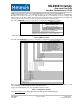
8.3.4 RAM
It is not possible to write into the RAM memory. It can only be read and only a limited number of RAM
registers are of interest to the customer.
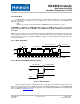
RAM (32x17)
Name Address Read access
Melexis reserved 0x00 Yes
… … …
Melexis reserved 0x03 Yes
Raw data IR channel 1 0x04
Raw data IR channel 2 0x05
T
A
0x06 Yes
T
OBJ1
0x07 Yes
T
OBJ2
0x08 Yes
Melexis reserved 0x09 Yes
… … …
Melexis reserved 0x1F Yes
Table 10: Ram addresses
8.4 SMBus compatible 2-wire protocol
The chip supports a 2 wires serial protocol, build with pins PWM / SDA and SCL.
SCL – digital input only, used as the clock for SMBus compatible communication. This pin has the
auxiliary function for building an external voltage regulator. When the external voltage regulator is used,
the 2-wire protocol is available only if the power supply regulator is overdriven.
PWM / SDA – Digital input / output, used for both the PWM output of the measured object
temperature(s) or the digital input / output for the SMBus. In PWM mode the pin can be programmed in
EEPROM to operate as Push / Pull or open drain NMOS (open drain NMOS is factory default). In
SMBus mode SDA is forced to open drain NMOS I/O, push-pull selection bit defines PWM / Thermal
relay operation.
SMBus communication with MLX90614 is covered in details in application notes, available from
www.melexis.com.
8.4.1 Functional description
The SMBus interface is a 2-wire protocol, allowing communication between the Master Device (MD)
and one or more Slave Devices (SD). In the system only one master can be presented at any given time [1].
The MLX90614 can only be used as a slave device.
Generally, the MD initiates the start of data transfer by selecting a SD through the Slave Address (SA).
The MD has read access to the RAM and EEPROM and write access to 9 EEPROM cells (at addresses
0x00, 0x01, 0x02, 0x03, 0x04, 0x05*, 0x0E, 0x0F, 0x09). If the access to the MLX90614 is a read operation it
will respond with 16 data bits and 8 bit PEC only if its own slave address, programmed in internal EEPROM, is
equal to the SA, sent by the master. The SA feature allows connecting up to 127 devices (SA=0x00…0x07F)
with only 2 wires, unless the system has some of the specific features described in paragraph 5.2 of reference
[1]. In order to provide access to any device or to assign an address to a SD before it is connected to the bus
system, the communication must start with zero SA followed by low R/W
¯
bit. When this command is sent from
the MD, the MLX90614 will always respond and will ignore the internal chip code information.
Special care must be taken not to put two MLX90614 devices with the same SA on the same bus
as MLX90614 does not support ARP [1].
The MD can force the MLX90614 into low consumption mode “sleep mode” (3V version only).
Read flags like “EEBUSY” (1 – EEPROM is busy with executing the previous write/erase), “EE_DEAD” (1 –
there is fatal EEPROM error and this chip is not functional**).