
Data Sheet


MP2636 –3.0A SINGLE CELL SW MODE BATTERY CHARGER WITH PPM AND 3.0A BOOST
MP2636 Rev.1.01 www.MonolithicPower.com 5
9/16/2015 MPS Proprietary Information. Patent Protected. Unauthorized Photocopy and Duplication Prohibited.
© 2015 MPS. All Rights Reserved.
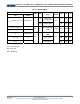
ABSOLUTE MAXIMUM RATINGS
(1)
VIN to PGND ................................-0.3V to +20V
SYS to PGND ..............................-0.3V to +6.5V
SW to PGND....................... -0.3V (-2V for 20ns)
.................................. To + 6.5V (8.8V for 20ns)
BATT to PGND ...............................-0.3V to +5V
ACOK
-----------------
, CHG
-------------
, BOOST
---------------------
to AGND
…... ..............................................-0.3V to +6.5V
All Other Pins to AGND................-0.3V to +6.5V
Continuous Power Dissipation (T
A
=+25°C)
(2)
........................................................... 2.97W
Junction Temperature...............................150ºC
Lead Temperature ....................................260ºC
Storage Temperature...............–65°C to +150ºC
Recommended Operating Conditions
(3)
Supply Voltage VIN............................4.5V to 6V
Battery Voltage BATT ..................2.5V to 4.35V
Operating Junction Temp (T
J
).. -40°C to +125°C
Thermal Resistance
(4)
θ
JA
θ
JC
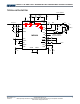
QFN-30 (4mmx4mm).............. 42 ........9.... °C/W
Notes:
1) Exceeding these ratings may damage the device.
2) The maximum allowable power dissipation is a function of the
maximum junction temperature T
J
(MAX), the junction-to-
ambient thermal resistance
JA
, and the ambient temperature
T
A
. The maximum allowable continuous power dissipation at
any ambient temperature is calculated by P
D
(MAX) = (T
J
(MAX)-T
A
)/
JA
. Exceeding the maximum allowable powe
r
dissipation will cause excessive die temperature, and the
regulator will go into thermal shutdown. Internal thermal
shutdown circuitry protects the device from permanent
damage.
3) The device is not guaranteed to function outside of its
operating conditions.
4) Measured on JESD51-7, 4-layer PCB.