
Data Sheet


MP2636 –3.0A SINGLE CELL SW MODE BATTERY CHARGER WITH PPM AND 3.0A BOOST
MP2636 Rev.1.01 www.MonolithicPower.com 39
9/16/2015 MPS Proprietary Information. Patent Protected. Unauthorized Photocopy and Duplication Prohibited.
© 2015 MPS. All Rights Reserved.
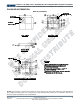
noise, efficiency and stability requirements. The
following design considerations can improve
circuit performance:
1) Route the power stage adjacent to their
grounds. Aim to minimize the high-side switching
node (SW, inductor) trace lengths in the high-
current paths.
Keep the switching node short and away from all
small control signals, especially the feedback
network.
Place the input capacitor as close as possible to
the VIN and PGND pins. The local power input
capacitors, connected from the SYS to PGND,
must be placed as close as possible to the IC.
Place the output inductor close to the IC and
connect the output capacitor between the
inductor and PGND of the IC.
2) For high-current applications, the power pads
for IN, SYS, SW, BATT and PGND should be
connected to as many coppers planes on the
board as possible. This improves thermal
performance because the board conducts heat
away from the IC.
3) The PCB should have a ground plane
connected directly to the return of all components
through vias (e.g., two vias per capacitor for
power-stage capacitors, one via per capacitor for
small-signal components). A star ground design
approach is typically used to keep circuit block
currents isolated (power-signal/control-signal),
which reduces noise-coupling and ground-
bounce issues. A single ground plane for this
design gives good results.
4) Place ISET, OLIM and ILIM resistors very
close to their respective IC pins.
IB
SW
SYS
VIN
VCC
ILIM
PWIN
TMR
BOOST
SW
SYS
VIN
CSP
BATT
VB
AGND
REG
FB
NTC
ISET
PGND
PGND
FREQ
EN
MODE
CHG
SYS
VIN
ACOK
OLIM
Figure 15: PCB Layout Guide