
Data Sheet


MP2636 –3.0A SINGLE CELL SW MODE BATTERY CHARGER WITH PPM AND 3.0A BOOST
MP2636 Rev.1.01 www.MonolithicPower.com 36
9/16/2015 MPS Proprietary Information. Patent Protected. Unauthorized Photocopy and Duplication Prohibited.
© 2015 MPS. All Rights Reserved.
APPLICATION INFORMATION
COMPONENT SELECTION
Setting the Charge Current in Charge Mode
In charge mode, both the external sense resistor,
RS1, and the resistor R
ISET
connect to the ISET
pin to set the charge current (I
CHG) of the MP2636
(see the Typical Application circuit).
Given expected I
CHG
and RS1, R
ISET
can be
calculated as:
ISET
CHG
2400
R(k)
I(A)RS1(m)
Ω=
×Ω
(11)
For example, for I
CHG
=2.5A, and RS1=20m,
R
ISET
= 48k.
Given a 20m RS1, the expected R
ISET
for typical
charge current listed as below:
R
ISET
(kΩ) Charge Current (A)
120 1.0
80 1.5
60 2.0
48 2.5
40 3.0
Setting the Input Current Limiting in Charge
Mode
In charge mode, connect a resistor from the ILIM
pin to AGND to program the input current limit.
The relationship between the input current limit
and setting resistor is as following:
ILIM
IN _LIM
43.3
R(k)
I(A)0.05
=Ω
+
(12)
For most applications, use R
ILIM
= 51k
(I
USB_LIM=900mA) for USB3.0 mode, and use R
ILIM
= 86.6k (I
USB_LIM
=500mA) for USB2.0 mode.
Setting the Input Voltage Range for Different
Operation Modes
A resistive voltage divider from the input to PWIN
pin determines the operating mode of MP2636.
PWIN IN
RL
VV (V)
RH RL
=×
+
(13)
If the voltage on PWIN is higher than 0.8V, the
MP2636 works in the charge mode. While the
voltage is lower than 0.8V, the MP2636 will work
in boost mode or sleep mode depending on the
MODE status. (see Table 1).
Setting the Input Voltage Regulation in
Charge Mode
In charge mode, connect a resistor divider from
the IN pin to AGND with tapped to REG pin to
program the input voltage regulation.
IN _ R REG
R3 R4
VV (V)
R4
+
=×
(14)
With the given R4, R3 is:
IN_ R REG
REG
VV
R3 R4(V)
V
−
=×
(15)
For a preset input voltage regulation value, say
4.75V, start with R4=5.1k, R3 is 15k.
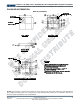
NTC Function in Charge Mode
Figure 14 shows that an internal resistor divider
sets the low temperature threshold (V
TL
) and high
temperature threshold (V
TH
) at 66.6%·V
SYS
and
35%·V
SYS
, respectively. For a given NTC
thermistor, select an appropriate R
T1
and R
T2
to
set the NTC window.
T2 NTC_Cold
TL
SYS T1 T2 NTC_Cold
R//R
V
TL 66.6%
VRR//R
===
+
(16)
T2 NTC_Hot
TH
SYS T1 T2 NTC_Hot
R//R
V
TH 35%
V R R //R
===
+
(17)
Where R
NTC_Hot
is the value of the NTC resistor at
the upper bound of its operating temperature
range, and R
NTC_Cold
is its lower bound.
The two resistors, R
T1
and R
T2
, independently
determine the upper and lower temperature limits.
This flexibility allows the MP2636 to operate with
most NTC resistors for different temperature
range requirements. Calculate R
T1
and R
T2
as
follows:
NTC_Hot NTC _ Cold
T1
NTC _ Cold NTC_Hot
RR (TLTH)
R
TH TL (R R )
×
×−
=
×× −
(18)
NTC_Hot NTC _ Cold
T2
NTC _ Cold NTC_Hot
RR (TLTH)
R
TH (1 TL) R TL (1 TH) R
×
×−
=
×− × − ×− ×
(19)
For example, the NCP18XH103 thermistor has
the following electrical characteristic:
At 0°C, R
NTC_Cold
= 27.445k;
At 50°C, R
NTC_Hot
= 4.16k.