
Data Sheet


MP2636 –3.0A SINGLE CELL SW MODE BATTERY CHARGER WITH PPM AND 3.0A BOOST
MP2636 Rev.1.01 www.MonolithicPower.com 10
9/16/2015 MPS Proprietary Information. Patent Protected. Unauthorized Photocopy and Duplication Prohibited.
© 2015 MPS. All Rights Reserved.
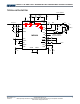
PIN FUNCTIONS
Pin # Name Description
1 IB
Charge Current Represent. The voltage at this pin indicates the charge current to the battery
in charge mode and discharge current out of the battery in boost mode.
2, 21 SW
Switch Output Node. It is recommended not to place Via’s on the SW plane during PCB
layout.
3, 20,
29
SYS
System Output. A minimum of 22μF ceramic cap is required to be put as close as
possible to the SYS and PGND pins. Total capacitance should NOT be lower than
44μF.
4, 19,
30
VIN Adapter Input. Place a bypass capacitor close to this pin to prevent large voltage spikes.
5 VCC
Internal Circuit Power Supply. Bypass this pin to GND with a 100nF ceramic capacitor. This
Pin CANNOT carry any external load.
6 ILIM
Input Current Set. Connect to GND with an external resistor to program input current limit in
charge mode.
7 PWIN
Input pin to detect the presence of valid input power. Pulling this pin to GND will turn off the
IN-to-SYS pass through MOSFET.
8 TMR
Oscillator Period Timer. Connect a timing capacitor between this pin and GND to set the
oscillator period for charge timer. Short to GND to disable the Timer function.
9 REG
Input voltage feedback for the input voltage regulation loop. Connect to tap of an external
resistor divider from VIN to GND to program the input voltage regulation. Once the voltage at
REG pin drops to the inner threshold, the charge current is reduced to maintain the input
voltage at the regulation value.
10
ACOK
----------------
Valid Input Supply Indicator. Logic LOW at this pin indicates the presence of a valid power
supply.
11 FB System Voltage Feedback Input.
12 NTC Negative Temperature Coefficient (NTC) Thermistor
13 ISET Charge Current Set. Connect an external resistor to GND to program the charge current.
14 OLIM
Programmable Output-Current Limit for Boost mode. Connect an external resistor to GND to
program the system current in Boost mode.
15 AGND Analog Ground
16 VB
Programmable Battery-Full Voltage. Connect to GND for 4.3V, leave floating to 4.35V, and
connect to logic HIGH for 4.2V.
17 BATT Positive Battery Terminal / Battery Charge Current Sense Negative Input.
18 CSP Battery Charge Current Sense Positive Input.
22
BOOST
---------------------
Boost operation indicator. Logic LOW indicates boost operation. The pin becomes an open
drain when the part operates at charge mode or sleep mode.
23
CHG
------------
Charging Completion Indicator. Logic LOW indicates charge mode. The pin becomes an
open drain once the charging has completed or is suspended.
24 MODE
Mode Select. Logic HIGHboost mode. Logic LOWsleep mode. Active only when ACOK
__________
is high (Input power is not available).