
Data Sheet


SD2405ALPI IIC 串行接口的实时时钟IC
!
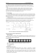
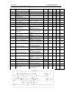
15. AC CHARACTERISTICS
SYMBOL
PARAMETER
CONDITIONS
MIN
TYP
MAX
UNITS
NOTES
V
IL
SDA and SCL input buffer LOW
voltage
-0.3
0.3×
V
DD
V
V
IH
SDA and SCL input buffer HIGH
voltage
0.7×V
D
D
V
DD
+0.3
V
Hyteresis
SDA and SCL input
buffer hysteresis
0.05×V
DD
V
V
OL
SDA output buffer LOW
voltage sinking 3mA
0
0.4
V
C
pin
SDA and SCL pin capacitance
T
A
=25℃ f=1MHZ
V
DD
=5V
V
IN
=0V V
OUT
=0V
10
pF
f
SCL
SCL frequency
400
kHZ
t
IN
Pulse width suppression time
at
SDA and SCL inputs
50
ns
t
AA
SCL falling edge to SDA
output data valid
SCL falling edge crossing
30%of
V
DD
until SDA exits the
30%to
70%of V
DD
window
900
ns
t
BUF
Time the bus must be free
before the start of a new
transmission
SDA crossing 70%of V
DD
during
a
STOP condition, to SDA
crossing
70%of V
DD
during the following
START condition
1300
ns
t
LOW
Clock LOW time
Measured at the 30% of
V
DD
crossing
1300
ns
t
HIGH
Clock HIGH time
Measured at the 70% of
V
DD
crossing
600
ns
t
SU:STA
START condition setup time
SCL rising edge to SDA
falling
edge Both crossing 70% of
V
DD
600
ns
t
HD:STA
START condition hold time
From SDA falling edge
crossing
30% of V
DD
to SCL falling
edge crossing 70% of
V
DD
600
ns
t
SU:DAT
Input data setup time
From SDA exiting the 30% to
70%
of V
DD
window ,to SCL rising
edge crossing 30% of
V
DD
100
ns
t
HD:DAT
Input data hold time
From SCL falling edge
crossing
30% of V
DD
to SDA entering
the
30% to 70%of V
DD
window
0
900
ns
t
SU:STO
STOP condition setup time
From SCL rising edge
crossing
70% of V
DD
,to SDA rising
edge crossing 30% of
V
DD
600
ns
t
HD:STO
Output condition hold time
From SDA rising edge to
SCL
falling edge .Both crossing 70%
of
V
DD
600
ns
t
DH
Output data hold time
From SCL falling edge
crossing
30% of V
DD
,until SDA enters
the
30% to 70% of V
DD
window.
0
ns
t
R
SDA and SCL rise time
From 30% to 70% of
V
DD
20+
0.1×Cb
300
ns
t
F
SDA and SCL fall time
From 70% to 30% of
V
DD
20+
0.1×Cb
300
ns
Cb
Capacitive loading of SDA
or
SCL
Total on-chip and off-chip
10
400
PF
R
PU
SDA and SCL bus pull-up
resistor off-chip
Maximum is determined by t
R
and
t
F For Cb=400pF,max is about
2~2.5k
Ω
For Cb=40pF,max is
about
15~20k
Ω
1
k
Ω