
Data Sheet
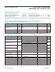

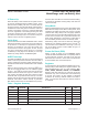
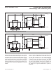

PIN
NAME FUNCTION
UCSP TDFN
A1 8 SDA
Serial Data Input/Output. Open-drain 2-wire data line. Connect this pin to the DATA signal of the
2-wire interface. This pin has a 0.2µA typical pulldown to sense disconnection.
A2 7 SCL
Serial Clock Input. Input only 2-wire clock line. Connect this pin to the CLOCK signal of the 2-wire
interface. This pin has a 0.2µA typical pulldown to sense disconnection.
A3 1 CTG Connect to Ground. Connect to VSS during normal operation.
B1 6 QSTRT Quick-Start Input. Allows reset of the device through hardware. Connect to GND if not used.
B2 N.C. No connect. Do not connect.
B3 2 CELL Battery Voltage Input. The voltage of the cell pack is measured through this pin.
C1 5
ALRT
Alert Output. Active-low interrupt signaling low state of charge. Connect to interrupt input of the
system microprocessor.
C2 3 V
DD
Power-Supply Input. 2.5V to 4.5V input range. Connect to system power through a decoupling
network. Connect a 10nF typical decoupling capacitor close to pin.
C3 4 GND Ground. Connect to the negative power rail of the system.
— — EP Exposed Pad (TDFN only). Connect to ground.
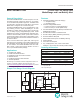
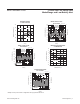
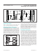
TOP VIEW
(BUMPS ON BOTTOM)
SDA SCL CTG
QSTRT
N.C. CELL
ALRT
V
DD
GND
+
UCSP
1 2 3
B
C
A
MAX17043
MAX17044
1
+
3 4
8 6 5
SDA
QSTRT ALRT
2
7
SCL
CTG V
DD
GNDCELL
TDFN
(2mm x
3mm)
TOP VIEW
MAX17043
MAX17044
MAX17043/MAX17044 1-Cell/2-Cell Fuel Gauge with
ModelGauge and Low-Battery Alert
www.maximintegrated.com
Maxim Integrated
│
5
Pin Description
Pin Congurations