
Data Sheet

8
Rev. A.02 www.3peakic.com.cn
LMV321A / LMV358A / LMV324A
80μA, 1.0MHz, Micro-Power Rail-to-Rail I/O Op Amps
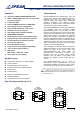
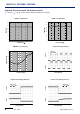
Pin Functions
-IN: Inverting Input of the Amplifier.
+IN: Non-Inverting Input of Amplifier.
OUT: Amplifier Output. The voltage range extends to
within mV of each supply rail.
V+ or +Vs: Positive Power Supply. Typically the voltage
is from 2.1V to 6.0V. Split supplies are possible as long
as the voltage between V+ and V– is between 2.1V and
6.0V. A bypass capacitor of 0.1μF as close to the part as
possible should be used between power supply pins or
between supply pins and ground.
V- or -Vs: Negative Power Supply. It is normally tied to
ground. It can also be tied to a voltage other than
ground as long as the voltage between V+ and V– is from
2.1V to 6.0V. If it is not connected to ground, bypass it
with a capacitor of 0.1μF as close to the part as
possible.
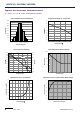
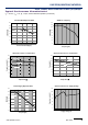
Operation
The LMV321A/358A/324A input signal range extends beyond the negative and positive power supplies. The output can
even extend all the way to the negative supply. The input stage is comprised of two CMOS differential amplifiers, a
PMOS stage and NMOS stage that are active over different ranges of common mode input voltage. The Class-AB
control buffer and output bias stage uses a proprietary compensation technique to take full advantage of the process
technology to drive very high capacitive loads. This is evident from the transient over shoot measurement plots in the
Typical Performance Characteristics.
Applications Information
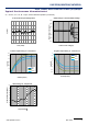
Low Supply Voltage and Low Power Consumption
The LMV321A/358A/324A of operational amplifiers can operate with power supply voltages from 2.1V to 6.0V. Each
amplifier draws only 80μA quiescent current. The low supply voltage capability and low supply current are ideal for
portable applications demanding HIGH CAPACITIVE LOAD DRIVING CAPABILITY and WIDE BANDWIDTH. The
LMV321A/358A/324A is optimized for wide bandwidth low power applications. They have an industry leading high
GBWP to power ratio and are unity gain stable for ANY CAPACITIVE load. When the load capacitance increases, the
increased capacitance at the output pushed the non-dominant pole to lower frequency in the open loop frequency
response, lowering the phase and gain margin. Higher gain configurations tend to have better capacitive drive
capability than lower gain configurations due to lower closed loop bandwidth and hence higher phase margin.
Low Input Referred Noise
The LMV321A/358A/324A provides a low input referred noise density of 27nV/√Hz at 1kHz. The voltage noise will
grow slowly with the frequency in wideband range, and the input voltage noise is typically 7μV
P-P
at the frequency of
0.1Hz to 10Hz.
Low Input Offset Voltage
The LMV321A/358A/324A has a low offset voltage tolerance of 400μV maximum which is essential for precision
applications. The offset voltage is trimmed with a proprietary trim algorithm to ensure low offset voltage for precision
signal processing requirement.
Low Input Bias Current
The LMV321A/358A/324A is a CMOS OPA family and features very low input bias current in pA range. The low input
bias current allows the amplifiers to be used in applications with high resistance sources. Care must be taken to
minimize PCB Surface Leakage. See below section on “PCB Surface Leakage” for more details.
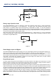
PCB Surface Leakage