
Data Sheet

10
Rev. A.02 www.3peakic.com.cn
LMV321A / LMV358A / LMV324A
80μA, 1.0MHz, Micro-Power Rail-to-Rail I/O Op Amps
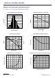
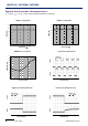
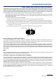
10kΩ
5pF
10kΩ
CPAR
VIN
VOUT
Figure 2
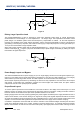
Driving Large Capacitive Load
The LMV321A/358A/324A of OPA is designed to drive large capacitive loads. Refer to Typical Performance
Characteristics for “Phase Margin vs. Load Capacitance”. As always, larger load capacitance decreases overall
phase margin in a feedback system where internal frequency compensation is utilized. As the load capacitance
increases, the feedback loop‟s phase margin decreases, and the closed-loop bandwidth is reduced. This produces
gain peaking in the frequency response, with overshoot and ringing in output step response. The unity-gain buffer (G =
+1V/V) is the most sensitive to large capacitive loads.
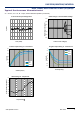
When driving large capacitive loads with the LMV321A/358A/324A (e.g., > 200 pF when G = +1V/V), a small series
resistor at the output (R
ISO
in Figure 3) improves the feedback loop‟s phase margin and stability by making the output
load resistive at higher frequencies.
VIN
VOUT
CLOAD
RISO
Figure 3
Power Supply Layout and Bypass
The LMV321A/358A/324A OPA‟s power supply pin (V
DD
for single-supply) should have a local bypass capacitor (i.e.,
0.01μF to 0.1μF) within 2mm for good high frequency performance. It can also use a bulk capacitor (i.e., 1μF or larger)
within 100mm to provide large, slow currents. This bulk capacitor can be shared with other analog parts.
Ground layout improves performance by decreasing the amount of stray capacitance and noise at the OPA‟s inputs
and outputs. To decrease stray capacitance, minimize PC board lengths and resistor leads, and place external
components as close to the op amps‟ pins as possible.
Proper Board Layout
To ensure optimum performance at the PCB level, care must be taken in the design of the board layout. To avoid
leakage currents, the surface of the board should be kept clean and free of moisture. Coating the surface creates a
barrier to moisture accumulation and helps reduce parasitic resistance on the board.
Keeping supply traces short and properly bypassing the power supplies minimizes power supply disturbances due to
output current variation, such as when driving an ac signal into a heavy load. Bypass capacitors should be connected
as closely as possible to the device supply pins. Stray capacitances are a concern at the outputs and the inputs of the
amplifier. It is recommended that signal traces be kept at least 5mm from supply lines to minimize coupling.
A variation in temperature across the PCB can cause a mismatch in the Seebeck voltages at solder joints and other
points where dissimilar metals are in contact, resulting in thermal voltage errors. To minimize these thermocouple
effects, orient resistors so heat sources warm both ends equally. Input signal paths should contain matching numbers