
Data Sheet

8
REV1.0 www.3peakic.com
TP5551
/
TP5552/TP5554
Ultra Low Noise, 3.5MHz, RRIO Zero-Drift Op-amps
Low Input Referred Noise
Flicker noise, as known as 1/f noise, is inherent in semiconductor devices and increases as frequency decreases. So
at lower frequencies, flicker noise dominates, causing higher degrees of error for sub-Hertz frequencies or dc precision
application.
The TP5551/2/4 amplifiers are chopper stabilized amplifiers, the flicker noise is reduced greatly because of this
technique. This reduction in 1/f noise allows the TP5551/2/4 to have much lower noise at dc and low frequency
compared to standard low noise amplifier.
Residual voltage ripple
The chopping technique can be used in amplifier design due to the internal notch filter. Although the chopping related
voltage ripple is suppressed, higher noise spectrum exists at the chopping frequency and its harmonics due to residual
ripple.
So if the frequency of input signal is nearby the chopping frequency, the signal maybe interfered by the residue ripple.
To further suppress the noise at the chopping frequency, it is recommended that a post filter be placed at the output of
the amplifier.
Broad Band And External Resistor Noise Considerations
The total broadband noise output from any amplifier is primarily a function of three types of noise: input voltage noise
from the amplifier, input current noise from the amplifier, and thermal (Johnson) noise from the external resistors used
around the amplifier. These noise sources are not correlated with each other and their combined noise can be
summed in a root sum squared manner. The full equation is given as:
221/2
[4 ( )]
nnsns
etotal e kTR i R
Where:
e
n
= the input voltage noise density of the amplifier.
i
n
= the input current noise of the amplifier.
R
S
= source resistance connected to the noninverting terminal.
k= Boltzmann’s constant (1.38x10
-23
J/K). T= ambient temperature in Kelvin (K).
The total equivalent rms noise over a specific bandwidth is expressed as:
,
nrms n
e e total BW
The input voltage noise density (en) of the TP555x is 55 nV/Hz, and the input current noise can be neglected. When
the source resistance is 190 k, the voltage noise contribution from the source resistor and the amplifier are equal.
With source resistance greater than 190 k, the overall noise of the system is dominated by the Johnson noise of the
resistor itself.
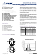
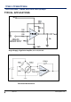
High Source Impedance Application
The TP5551/2/4 uses switches at the chopper amplifier input, the input signal is chopped at 125kHz to reduce input
offset voltage down to 10µV. The dynamic behavior of these switches induces a charge injection current to the input
terminals of the amplifier. The charge injection current has a DC path to ground through the resistances seen at the
input terminals of the amplifier. Higher input impedance cause an apparent shift in the input bias current of the
amplifier.
Because the chopper amplifier has charge injection currents at each terminal, the input offset current will be larger
than standard amplifiers. The Ios of TP5551/2/4 are 150pA under the typical condition. So the input impedance should
be balanced across each input(see Figure xx). The input impedance of the amplifier should be matched between the
IN+ and IN- terminals to minimize total input offset current. Input offset currents show up as an additional output offset
voltage, as shown in the following equation: