
Data Sheet
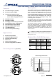

3
TP5551
/
TP5552/TP5554
Ultra Low Noise, 3.5MHz, RRIO Zero-Drift O
p
-am
p
s
www.3peakic.com REV1.0
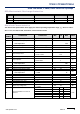
ESD, Electrostatic Discharge Protection
Symbol Parameter Condition Minimum Level Unit
HBM Human Body Model ESD MIL-STD-883H Method 3015.8 7 kV
CDM Charged Device Model ESD JEDEC-EIA/JESD22-C101E 2 kV
Electrical Characteristics
The denotes the specifications which apply over the full operating temperature range, T
A
= -40°C to +125°C .
At T
A
= 27°C, V
DD
=5V, R
L
=10K, Vcm=V
DD
/2, unless otherwise noted.
VDD=5V,
SYMBOL
PARAMETER CONDITIONS MIN TYP MAX UNITS
V
DD
Supply Voltage Range 1.8 5.5 V
I
Q
Quiescent current per amplifier I
O
= 0 500 590
A
Over temperature 820
V
OS
Input Offset Voltage Input grounded, unity gain. ±1 ±5 V
dV
OS
/dT vs. Temperature 0.008 0.05 V/°C
PSRR vs. Power Supply V
S
= +1.8V to +5.5V 0.5 V/V
V
N(P-P)
Input Voltage Noise
f = 0.01Hz to 1Hz 0.1
V
PP
f = 0.1Hz to 10Hz 0.35
V
N
Input Voltage Noise Density f = 1kHz 15 nV/Hz
C
IN
Input Capacitor
Differential 3
pF
Common-Mode 2
I
B
Input Current ±50 ±200
pA
Over temperature 800
I
OS
Input Offset Current ±100 ±400 pA
V
CM
Common-mode Voltage Range (V-)-0.1 (V+)+0.1 V
CMRR Common-mode Rejection Ratio 110 130 dB
V
O
Output Voltage Swing from Rail R
L
= 10k 5 10
mV
Over temperature R
L
= 10kΩ 10
I
SC
Short-circuit Current ±60 mA
C
L
Maximum Capacitive Load 1000 pF
GBW Unity Gain Bandwidth C
L
= 100pF 3.5 MHz
SR Slew Rate G = +1, C
L
= 100pF 2.5 V/s
t
OR
Overload Recovery Time G = -10 35 s
t
S
Settling Time to 0.01% C
L
= 100pF 20 s
A
VO
Open-Loop Voltage Gain
(V-)+0.1V < V
O
< (V+)-0.1V,
R
L
= 100k
100 120 dB
JA
Thermal Resistance Junction to
Ambient
SOT23-5 200
°C/W
MSOP-8 210
SO-8 158
SC70-5 250
SO-14 83
TSSOP-14 100